Sony’s Triple-Layer Image Sensor Promises Huge Performance Gains
Sony Imaging and Sensing Solutions (I&SS) segment recently held a chat with investors, and as part of its presentation, Sony Semiconductor Solutions (SSS) expanded upon a prospective triple-layer image sensor that promises significant performance improvements.
As spotted by Sony Alpha Rumors, the presentation covers the company’s FY2024 performance — which saw record-high sales and operating income — and Sony’s broader development plans.
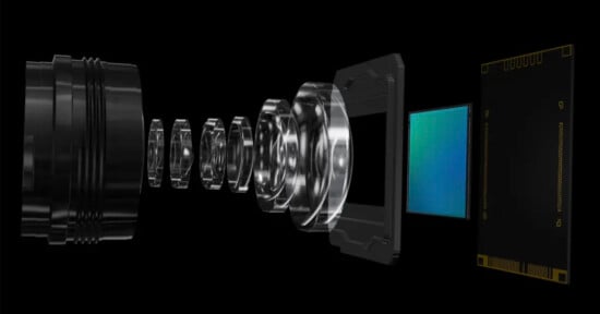
As part of its long-term goals, Sony is investing heavily in new sensor technology, including improved multi-layer stacked image sensors. Sony already uses stacked sensors in many cameras, including the flagship a1 II, but these are two-layer sensors. There is a photodiode layer, which includes all the pixels that capture photos, and a second, lower transistor layer that handles processing tasks.
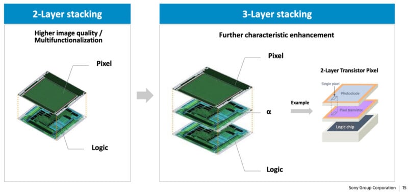
Sony’s long-term ambitions to add a third layer to the image sensor stack essentially means expanded processing and improved image quality. The more processing power at the sensor level, the better, all else equal.
As Sony explains, enhanced processing power at the sensor level can improve apparent dynamic range, sensitivity, noise performance, efficiency, readout speed, and resolution, although this last advantage applies more to video performance than to still images. Another sensor layer doesn’t itself change resolution, but by making a sensor faster and more performant, it could unlock new video recording modes. High-resolution image sensors are now typically limited in terms of video resolution by processing bottlenecks, so removing or reducing those could unlock additional video performance.
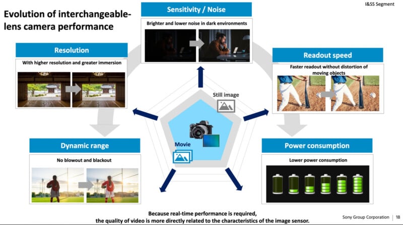
Better readout speed is excellent for nearly every aspect of a camera’s performance, including with rolling shutter, continuous shooting speeds, and autofocus performance.
Hypothetical dynamic range benefits are complicated. Better sensor-level image processing can help apparent dynamic range, but a sensor’s actual dynamic range depends on many factors, including the full-well capacity of a sensor’s pixels and sensor-level noise performance. While processing impacts noise, full-well capacity is a physical situation with the actual pixels, and adding more layers to a sensor can actually reduce full-well capacity by physically shrinking the pixels.
However, Sony explained this situation way back in 2021 when it unveiled initial concepts of a triple-layer image sensor. As Sony demonstrated previously, the third layer can also be pixel transistors located below the photodiode layer rather than a second pure processing layer.
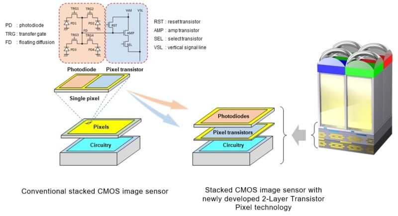
“Sony’s new architecture is an advancement in stacked CMOS image sensor technology that separates the photodiodes and pixel transistors onto separate substrates that are stacked on top of each other, rather than side-by-side,” PetaPixel wrote in late 2021. “Sony says that the new stacking technology enables the adoption of architectures that allow the photodiode and pixel transistor layers to each be optimized, thereby approximately doubling saturation signal level relative to conventional image sensors and, in turn, widening dynamic range.”
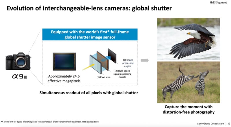
When such a sensor may arrive in an Alpha or FX-series product remains an open question, but Sony Semiconductor Solutions has proven time and again that it can make groundbreaking image sensors, such as the global shutter sensor in the a9 III and the fast, high-res stacked sensor in the a1 series. Sony remains very committed to full-frame image sensor development, and the future looks bright.
Image credits: Sony