Sony Says Its New Sensor Has Way Better Dynamic Range With Less Noise
Last year, Sony said that it had developed a new type of sensor that was capable of gathering double the light of conventional sensors while also reducing noise. That sensor has finally made it into a consumer product, and the company has further explained how it works.
Back in December 2021, Sony claimed that it had designed a new sensor that was able to dramatically redesign an image sensor with what it claimed resulted in majorly improved imaging. According to the company, typical image sensors place photodiodes and pixel transistors on the same substrate, but in this new design, Sony was able to separate them onto different substrate layers.
The result was a sensor that approximately doubled its light gathering capability.
The following February, Sony went into further detail on how it made this sensor, but the explanations for how this technology worked were previously only available translated from Japanese. However, today Sony has taken a page out of Samsung’s book and shared a new animated video that explains the technology succinctly.
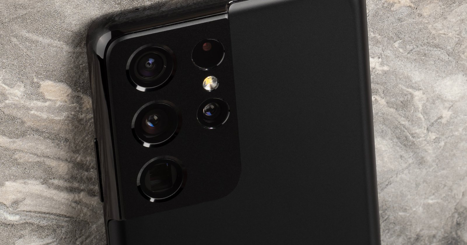
The sensor is found in the new Xperia 1 V smartphone that was announced earlier this week and while its physical size doesn’t sound that impressive on paper — it’s notably smaller than the Type 1 (also called 1-inch) sensor that is usually the baseline expectation for high image quality — Sony says that it is an extremely capable technology that skyrockets dynamic range to a level that “has never been seen before in smartphones” while also upping the low-light performance.
“This new technology will prevent underexposure and overexposure in settings with a combination of bright and dim illumination (e.g., backlit settings) and enable high-quality, low-noise images even in low-light (e.g., indoor, nighttime) settings,” Sony says.
![]()
The sensor was produced under Sony’s LYTIA brand, which specializes in smartphone imagers.
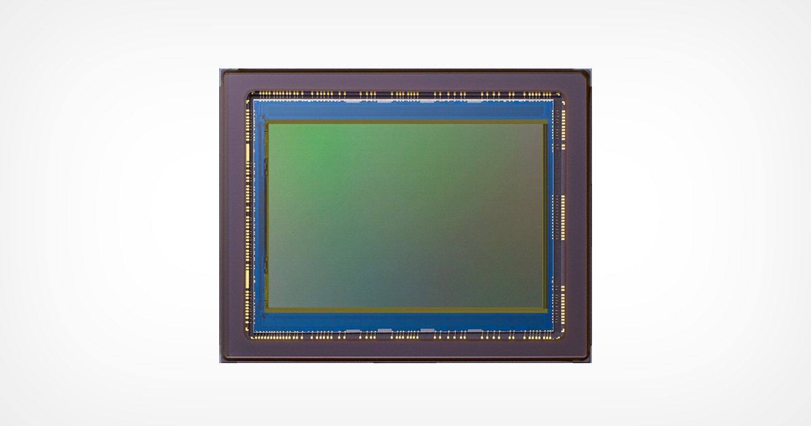
![]()
“The new technology, with approximately double the saturation signal level relative to conventional image sensors, has succeeded in widening the dynamic range—the range of dark-to-bright tones that can be recorded by a camera. This will enable the image sensor to produce images that reduce overexposure and underexposure in settings with a combination of bright and dim illumination, without increasing the size of the image sensor, achieving images closer to the way they are perceived through the human naked eye,” Sony claims.
stacked CMOS image sensor
stacked CMOS image sensor
Sony says that typically adjusting exposure in dimly lit settings usually only results in brighter images in exchange for more noise. This new sensor reduces that tradeoff.
“By increasing the size of the amp transistors, the 2-Layer Transistor Pixel technology has succeeded in substantially reducing noise which can affect images taken in dark settings. High-quality, low-noise indoor, nighttime, and other dark-location images are now possible thanks to this technology, without having to increase the size of the image sensor,” the company claims.
“[The] 2-Layer Transistor Pixel stacked CMOS image sensor makes it possible to shoot night sky and human skin with low noise.”
The new sensor is currently only available on Sony’s upcoming Xperia 1 V smartphone, but given how excited the company is about the technology and the claims it makes about image quality improvement, expect to see it rolled out to other smartphone makers in the future.