Sony Explains How Its Groundbreaking 2-Layer CMOS Sensor Was Made
In December of 2021, Sony successfully developed the world’s first stacked CMOS image sensor technology with two-layer transistor pixels, doubling its light gathering capability. The company has now further detailed how this was achieved.
The Revolutionary Sensor
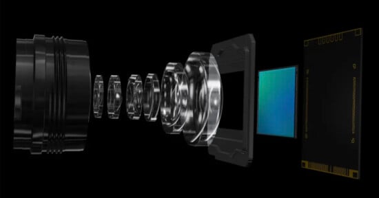
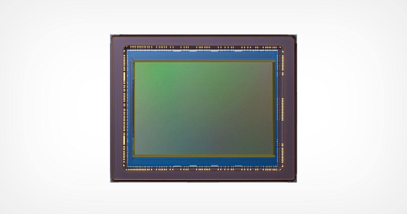
As explained in PetaPixel’s initial coverage, Sony’s new sensor separates the photodiodes and pixel transistors that are normally placed on the same substrate onto different substrate layers. The result is a sensor that approximately doubles the saturation signal level — basically its light gathering capability — which dramatically improves the dynamic range and reduces noise.
Sony specifically notes that this technology is going to make for increasingly high-quality imaging in the case of smartphone photography without necessarily increasing the size of the smartphone sensor. The new technology’s pixel structure will enable pixels to maintain or improve their existing properties at not only current but also smaller pixel sizes.
Sony Shares Details Behind the Sensor’s Creation
The new information is found in a new video that was originally captured on January 25, 2022 as part of the All Sony Semiconductor Solutions (SSS) Group Event, “Sense the Wonder Day”, spotted by Sony Alpha Rumors.
Keiichi Nakazawa of Sony Semiconductor’s Second Research Division, explains the new sensor as well as how Sony was able to create it. Nakazawa is in charge of research and development of new image sensors for mobile, which is in line with why Sony’s new technology is such a breakthrough for smaller sensors.
Nakazawa says that while developing the new structure, his team’s goal was initially to create the ultimate pixel structure and what that would actually mean.
“During this discussion, we came to the conclusion that both photo diodes and transistors must give the best performance,” he says. “This led to the concept of the two-layer transistor pixel.”
![]()
Nakazawa says the result is a sensor that has been well-received and has high expectations.
“Because the photo diodes and pixel transistor are physically separated in this structure, it has become possible to optimize each of them. The announcement mentioned expected pixel performance improvements such as enhanced dynamic range and noise improvements. However, the device has many possibilities for additional new functions, as well as performance improvements. Various studies are underway at the R&D organization for this.”
One detail that Nakazawa reveals about the process was a major challenge involved in the heat needed to create the new bonds.
“This technology enables the stacked devices to connect different substrates to a single pixel unit. This requires an alignment technology with nanometer accuracy for the photo diodes and pixel transistors. To realize this, a process technology called 3D sequential integration was adopted. Instead of conventional bonding of completed wafers, new wafers are bonded together during the production flow.
“Specifically, after the photo diode is formed, silicon wafers are bonded and a process technology for forming pixel transistors is used. This means that the alignment accuracy is determined by the lithography, not the bonding, and a highly accurate alignment is realized,” he explains.
“A major issue with this technology is the heat in the production process after stacking the wafers. Whereas the heat resistance for bonding technology in conventional structures is 400-degrees Celcius, this new structure requires a heat resistance of over 1,000-degrees Celcius,” he continues.
“To solve this problem, we evolved our bonding technology and transistors have been built to adapt to this structure.”
Sony has not said when the new sensor can be expected in consumer devices nor when it plans to manufacture it at scale, but has said that it will continue to iterate on the design going forward.