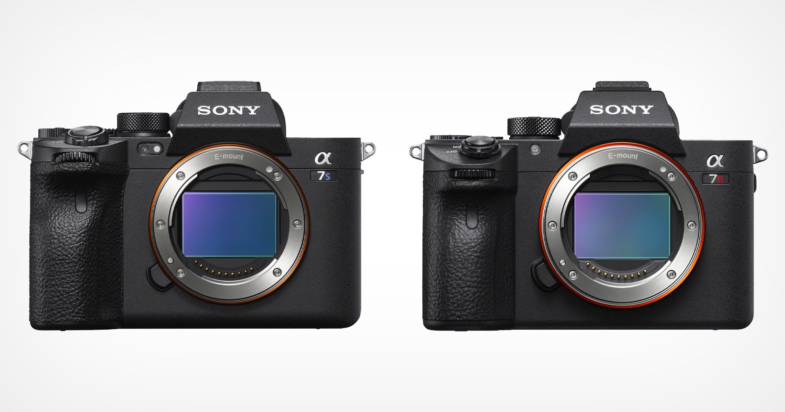
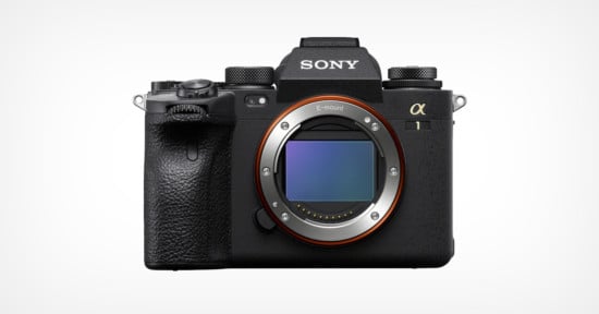
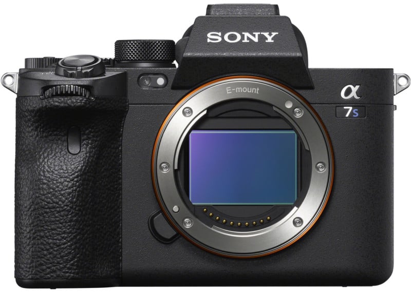
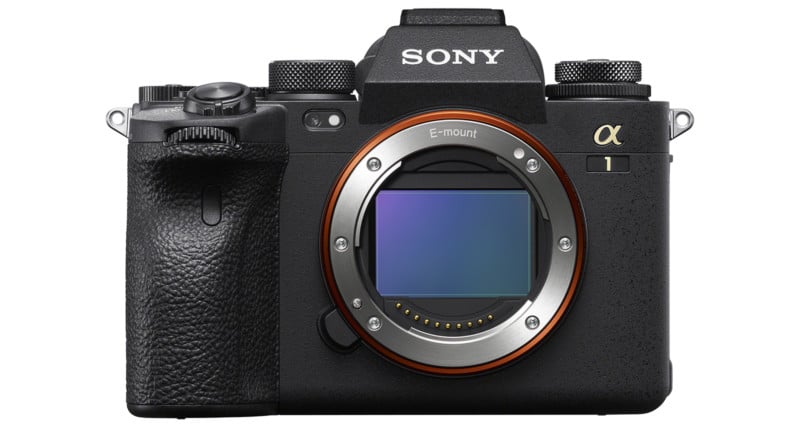
Could the Alpha 7S III be Using the Same Sensor as the Alpha 1?
A teardown by astrophotography site LandingField found that the 12-megapixel Alpha 7S III is using four photosites to create a single pixel, meaning its actual resolution is 48-megapixels. Some have taken this to mean that it uses the same sensor as the Alpha 1.
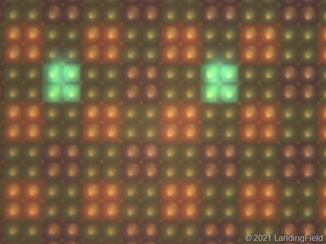
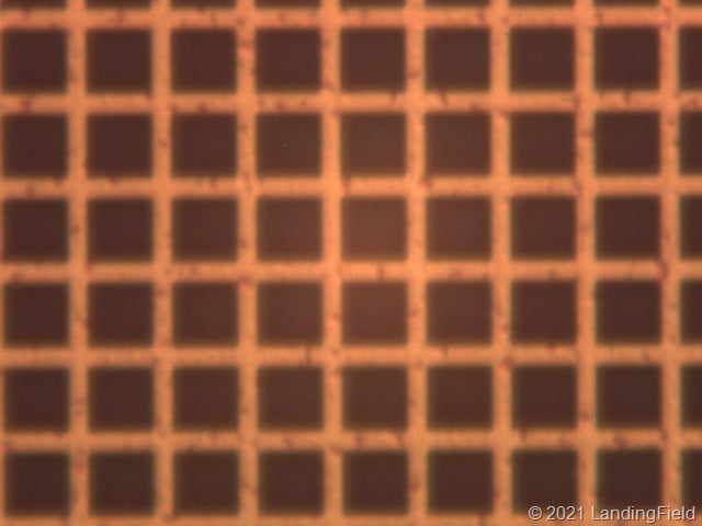
After tearing down the sensor and examining it under a microscope, Landingfield discovered that the sensor uses what the publication describes as a “2×2 binning” design, which leads to the conclusion that the sensor in the camera — the IMX510 — actually has a 48-megapixel native resolution.
The RGGB Bayer pattern is spread across a 4×4 grid. After sensor readout, the four pixels in each of the same color are then combined digitally to give one pixel before sending out on the SLVS-EC interface. This could explain the increase in read noise. From my knowledge, none of Sony DSLR CIS supports charge binning due to limitation in its pixel architecture. By combining four pixels digitally, you would increase the noise variance by four and hence read noise almost doubles (sqrt to RMS).
This assertion brings up a major question: would what is happening here be binning or oversampling? “Pixel binning” is described as using a set of adjacent pixels to create a single pixel while oversampling is described as using multiple full-size pixels to create one larger pixel. It sounds like semantics, but Sony actually specifically writes that the Alpha 7S III does not have pixel binning in its press materials during the launch of the camera, meaning the accusation of binning is rather significant.
Specifically, Sony definitively stated that the Sony Alpha 7S Mark III has no pixel binning or line skipping. Sony’s legal team would be unlikely to green-light this statement if the camera did in fact actually pixel bin. It might come down to what Sony’s engineers define as “binning” or “oversampling.”
PetaPixel reached out to Sony, but the company did not immediately respond. As a rule, however, Sony does not provide information on its engineering designs, so it’s unlikely the answer to these questions would come from the company direclty.
Few experts on sensor engineering exist outside of those who work for the camera companies, but Imaging Resource’s founder Dave Etchells is one of them. PetaPixel asked him to provide some of his thoughts on the topic.
“It’s binning but in a different sense than what people have conventionally called binning,” he tells PetaPixel after taking a look at LandingField’s report. “It’s binning digitally which is different than oversampling as well. Normally when we say binning that means that they are taking the actual charge that is collected by each pixel and combining it to a larger charge before reading it out [which isn’t happening here].”
Etchells says that one way to think about this is to think of the individual pixels as cups of water and the capacitor as a larger cup — rudimentary, but illustrative. With binning, think of those cups of water as being dumped into the larger cup and then measured. What Sony is doing here is instead of that, the cups are being individually measured and not dumped into a larger cup at all.
“What Sony appears to be doing on this sensor is they measure each of the little ‘cups’ and then adds those numbers together. So the charge is combining the numbers as it is being read out,” he says.
“Sony is reading the voltage on each individual capacitor and adding the numbers together. So it’s not technically binning. It has the same resolution consequences the way binning does, but you also actually get a worse signal-to-noise ratio than if you did bin,” he explains.
Looking back at the cups analogy, Etchells says it’s kind of like reading imagining that there are measurement lines on each of the individual cups and that there is some level of inaccuracy associated with those lines if someone were to eyeball pouring liquid into those cups to measure them. Whether those lines are on each small cup or on the larger cup, there is some level of uncertainty in reading it. If someone was to dump all the liquid of the small cups into one big cup and then read it, there would be just one amount of error. But if you have four little cups that are being measured individually instead, that is four possible errors that are being combined together.
“Sony isn’t binning in the traditional sense, but they are taking the signals out of a group of four pixels and measuring them and combining those together before they get sent on to the processor. It’s the same as binning from the standpoint that you’re losing resolution, but it’s different from binning in that you’re probably also getting more noise,” Etchells says. “They’re combining four individual measurements of pixel voltage and that basically means you have twice as much readout noise.”
Some have taken the structure of the sensor to mean that Sony used the same sensor — or some derivation of it — in the Alpha 7S III as it did in the Alpha 1, since the Alpha 1 offers full-width 4K video capture with pixel binning from 48 million photosites. If Landingfield’s information is correct, this is what was found on the Alpha 7S III, but the binning is instead hard-wired into the sensor.
Etchells says this does make some sense, as it would be a relatively minor change to adjust how the company was reading a sensor versus designing entirely new pixels and would explain why the company went with a route that actually introduced more noise than traditional pixel binning would. This is also one theory that LandingField’s report comes to as to why Sony would go with this design.
The other theory as to why Sony would do this is that for HDR, there is potentially a really big advantage in that each pixel can have different sensitivities. By varying the sensitivity on each pixel it would give them more dynamic range, in theory, Etchells says.
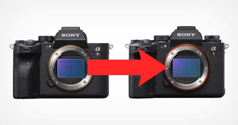
Both the Alpha 1 and the Alpha 7S III have 759 phase-detection autofocus points, which may lend credence to the idea that both use variations of the same sensor. But on the flipside, four pixels making up one pixel in the 12-megapixel Alpha 7S III would mean 48-megapixels, which is fewer than the Alpha 1’s 50-megapixels. That could mean the sensors are different, but one could argue that Sony might just be cropping the Alpha 7S III sensor a bit.
So are both cameras using variations on the same sensor? Probably not, but it’s inconclusive without more information.
“Based on the recorded pixel pitch (Alpha 7S III is 8.4 versus the Alpha 1’s 4.16), There is about a 2% difference and so I strongly suspect they’re not the same chip since it’s not exactly divisible into each other. But that depends on if we’re looking at actual pixel dimensions published by Sony or if we’re just dividing sensor size by the number of pixels,” Etchells continues.
He also says this is assuming that the two cameras have exactly the same framing.
“If it turns out that the Alpha 7S III is cropped just slightly tighter, I would then argue strongly that it was the same chip. It would be interesting to have both cameras locked down with the same lens to see where the edges of the frame would be.”
The full breakdown of the sensor can be seen on LandingField, which it should be noted never specifically asserts that the sensor shares anything in common with the Alpha 1. Still, it is worth considering what the company defines as pixel binning or oversampling and thinking about what this means as far as sensor development.