Canon is Making Metalenses, Further Legitimizing the Technology

Metalenses are a relatively fringe optical technology — at least, they were. Until now, it has been largely pursued by startups and scientists but that is changing as Canon has jumped into the fray and not only makes them but also produces the equipment necessary to manufacture them.
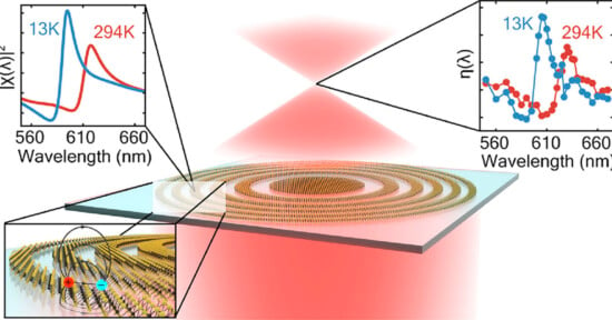
Metalenses are flat surfaces that are designed to replace full-size optics with a wholly different method. Basically, metalenses reduce the typically large and complicated optical structure of a standard camera lens and compress it into a much smaller system that bends light using nanoparticles and metasurfaces instead of curved optics. The goal of a metalens would be to, eventually, wholly eliminate the smartphone camera bump.
This technology is very new — it was only two years ago that scientists from MIT managed to create a prototype metalens that was able to adjust focus without any moving parts.
The biggest players in the field are a company called Metalenz and Samsung, although the latter has only mentioned it was interested in pursuing the technology for use in smartphones — a common goal given that camera systems on smartphones are a notable area that is becoming increasingly difficult to downsize using traditional optics. Metalenz, on the other hand, is working directly in the research and manufacturing of metalenses and is perhaps the biggest name in the space. The startup closed Series B funding last October with an additional $30 million funding round, highlighting the interest in the technology.
Japanese publication Mynavi News reports that Canon showcased its support for metalens technology during its Canon Expo 2023, a private exhibition by the Canon Group where it shows off its latest technology. Historically, a large percentage of new technological innovations shown at Canon Expos have gone on to become market-facing within a short period of time — often in as little as a couple of years.

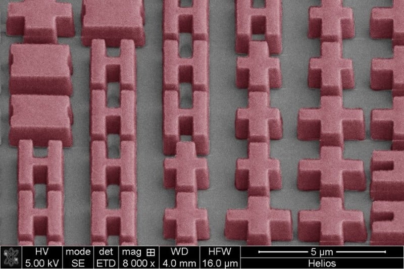
That is what makes Canon’s metalens showcase particularly intriguing. Canon is a massive company whose interest in any technology segment has the ability to dramatically change it. Not only does Canon have a prototype metalens, as shown in photos by Mynavi News, it was produced using the company’s latest nanoimprint manufacturing system that it announced earlier this month.
Canon is not only producing metalenses, but it is producing them with hardware it also makes. This level of investment in a technology and the fact it is being showcased at Canon Expo all but confirms the company plans to move forward in this space with considerable investment. With a big player like Canon now in the field, metalens technology — which hasn’t proven itself to be viable in consumer devices yet — is not only more legitimate as a business endeavor but also the likelihood it starts to show up in devices feels far closer than it did just a few weeks ago.
Oddly, Canon declined to provide PetaPixel with detailed information about its metalens technology and also chose not to provide any photos of its tech. The only images that are available are in the Mynavi News article.