Canon Develops Tool Critical for Making Advanced Semiconductors

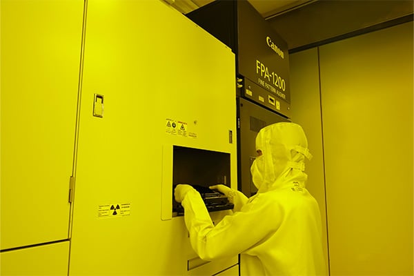
Canon is expanding even further outside of imaging with the release of a new nanoimprint semiconductor manufacturing device capable of executing circuit pattern transfer, a critical tool needed to make the most advanced semiconductors.
While known mainly for cameras and lenses, Canon does have its hands in other industries outside of imaging including semiconductor manufacturing. As CNBC reports, the addition of this new machine, called the FPA-1200NZ2C, allows it to challenge the market leader in extreme ultraviolet (EUV) lithography (Dutch firm ASML). This new Canon machine is capable of making semiconductors that are equivalent to a 5-nanometer process and can go as small as 2 nanometers.
“Canon’s NIL technology enables patterning with a minimum linewidth of 14 nm, equivalent to the 5-nm-node required to produce most advanced logic semiconductors that are currently available. Furthermore, with further improvement of mask technology, NIL is expected to enable circuit patterning with a minimum linewidth of 10 nm, which corresponds to 2-nm-node,” the company says.
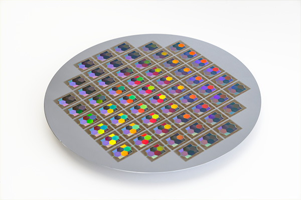
The FPA-1200NZ2C works differently than other photolithography equipment, too. Instead of transferring a circuit pattern by projecting it onto the resist-coated wafer, Canon’s new solution does it by pressing a mask imprinted with the circuit pattern on the resist on the wafer — like a stamp.
“Because its circuit pattern transfer process does not go through an optical mechanism, fine circuit patterns on the mask can be faithfully reproduced on the wafer. Thus, complex two- or three-dimensional circuit patterns can be formed in a single imprint, which may reduce the cost of ownership (CoO),” Canon says.
CNBC adds that, for context, the A17 Pro chip inside the new iPhone 15 Pro and Pro Max is a 3nm semiconductor. TSMC and Samsung — behemoths in the advanced chip manufacturing sector — are planning to make 2nm chips by 2025. Canon, therefore, is well-positioned to support them with the FPA-1200NZ2C.
That said, Canon’s nanoimprint lithography — a technology it has been working on since 2004 — hasn’t taken off widely since the type of machine developed by ASML has worked better during the chip printing process. Canon, clearly, hopes that will change with this new device.
“The new product employs newly developed environment control technology that suppresses the contamination with fine particles in the equipment,” Canon says.
“This enables high-precision alignment which is necessary for the manufacture of semiconductors with an increasing number of layers and the reduction of defects due to fine particles, and enables the formation of fine and complex circuits, contributing to the manufacture of cutting-edge semiconductor devices.”
Image creditsHeader photo licensed via Depositphotos.