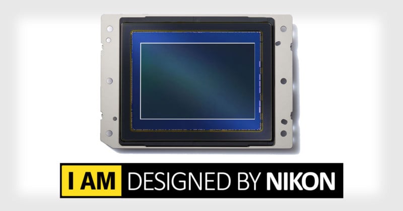
Yes, Nikon Designs Its Own Sensors
Sony has been receiving attention and praise in recent years for the quality of its sensors and the fact that it produces sensors for other heavyweight camera companies, including Nikon. But even though some of Nikon’s CMOS sensors may be manufactured in Sony factories, Nikon actually spends a considerable amount of resources designing those high-end sensors.
“I’ve known for some time that Nikon actually designs their own sensors, to a fairly minute level of detail,” Etchells writes. “I think this is almost unknown in the photo community; most people just assume that ‘design’ in Nikon’s case simply consists of ordering-up different combinations of specs from sensor manufacturers, picking a feature from column ‘A’, another from column ‘B’ and so on, like a Chinese restaurant menu.
“In actuality, they have a full staff of sensor engineers who design cutting-edge sensors like those in the D5 and D850 from the ground up, optimizing their designs to work optimally with NIKKOR lenses and Nikon’s EXPEED image-processor architecture.”
Responsible for determining the layout of devices on the CMOS sensor, Nikon’s sensor designers (assembled in teams that work on sensors for specific cameras) work to create an optimal combination of light-gathering efficiency, noise levels, readout speeds, power consumption, and more.
“One of the most surprising things to me was how much time they spent designing and testing for how the sensors interact with their optics,” Etchells tells PetaPixel. “That had never occurred to me as a thing before, but they seem to put in a lot of cycles on it.”
“Makes sense, [since] light doesn’t just appear at the sensor — the LPF, IR filter, microlenses and what’s under the microlenses are all part of an optical system that starts with the lens.”
“Even though I knew that Nikon had its own sensor design operation, I was surprised to learn just how deep the process runs,” writes Etchells, who holds a Master’s in semiconductor physics. “[T]he level of design, simulation and testing I saw was frankly astonishing.”
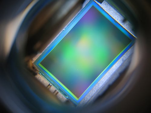
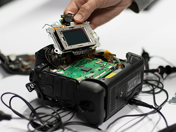
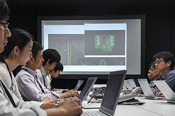
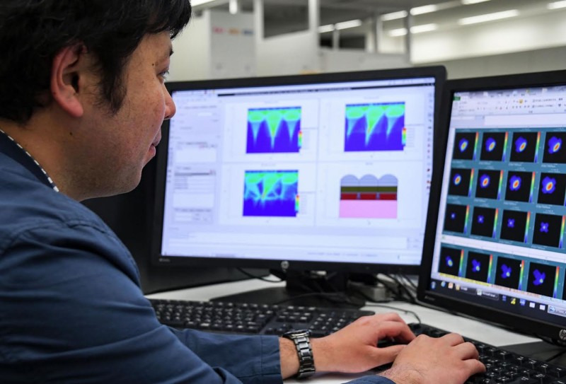
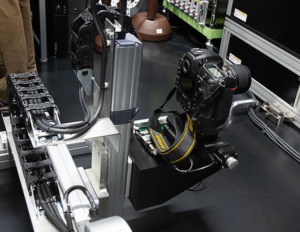
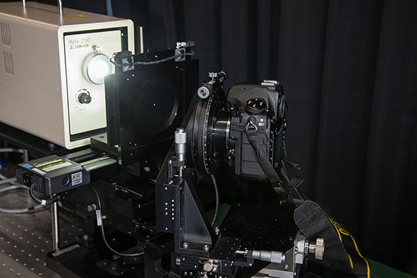
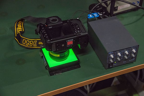
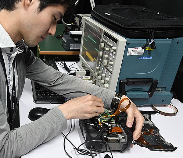
Steps include sensor/lens testing, angle of incidence testing, RGB testing, and in-circuit testing. Here are some views of the tests in action (Etchells also has videos of them being performed in his report):
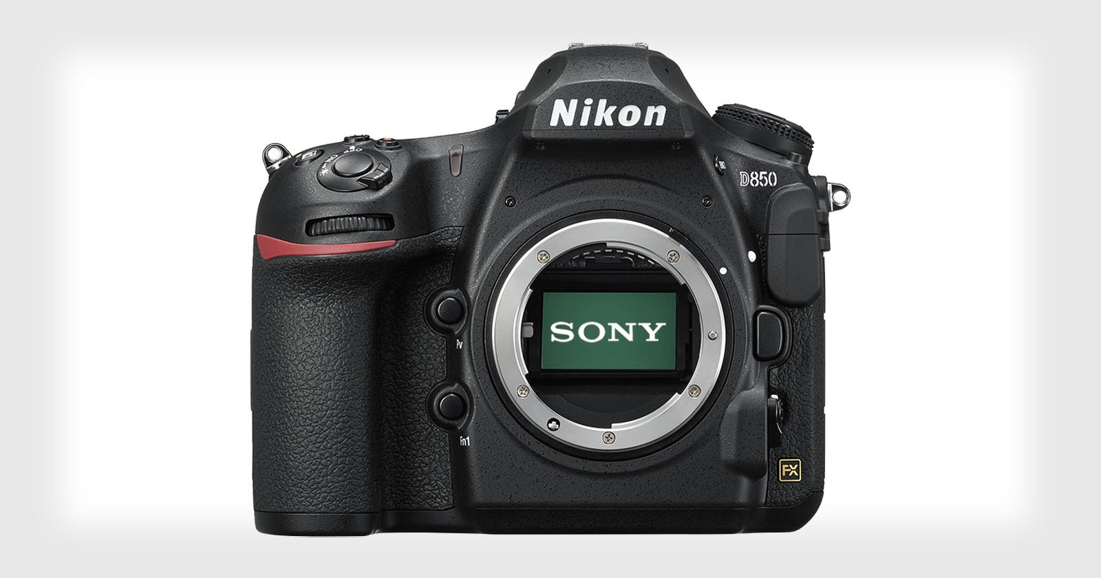
Nikon has long touted the fact that the highly-reviewed sensor in the Nikon D850 was designed entirely in-house, but Sony stole some of Nikon’s thunder back in June when it was found that the D850 sensor has a Sony-style model number hidden on the back.
But Nikon fans, rest assured: it was Nikon minds and hands that developed the sensor from the ground up.
Etchells’ full report from his time with Nikon’s sensor designers weighs in at nearly 8,000 words. Head on over to Imaging Resource if you’d like to read the technical details of what the engineers do.
Image credits: All photos and videos by Dave Etchells/Imaging Resource and used with permission