Sony a7R II Teardown Gives Us an Inside Look at the Mirrorless Beast
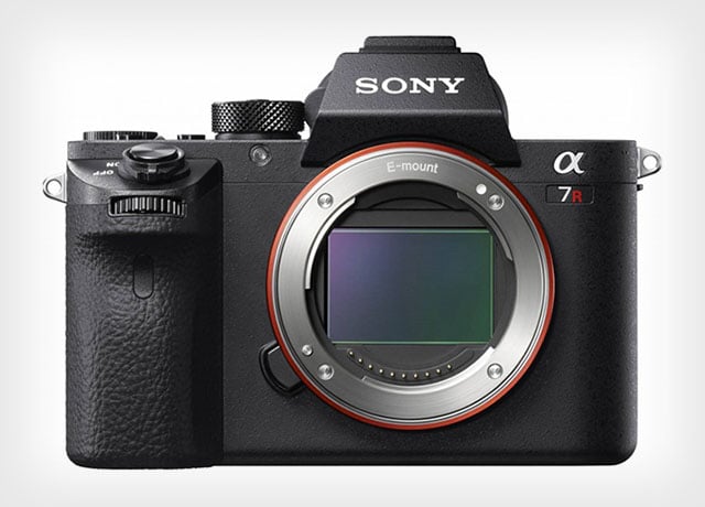
One camera that has generated a great deal of interest in recent days is the Sony a7R II, which packs the world’s first BSI full-frame sensor, ISO 102400, and 4K video into a flagship mirrorless body.
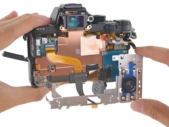
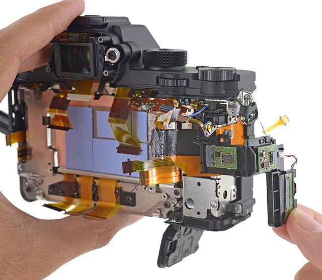
The folks over at iFixit have just published a teardown of the a7r II, giving us a glimpse into the guts of the highly-anticipated camera body.
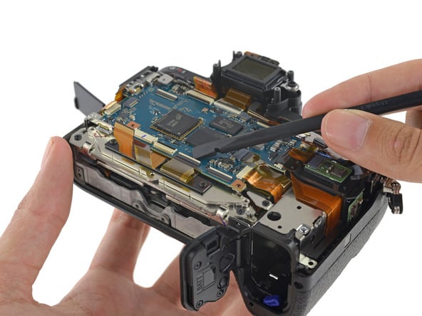
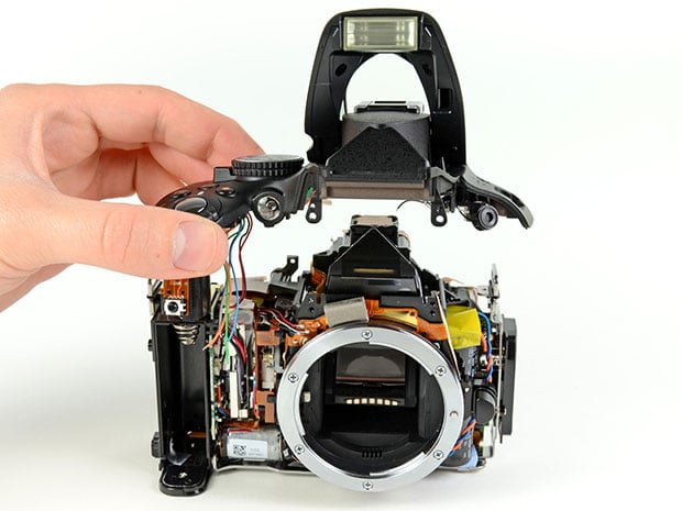
Removing the motherboard and the processor chips:
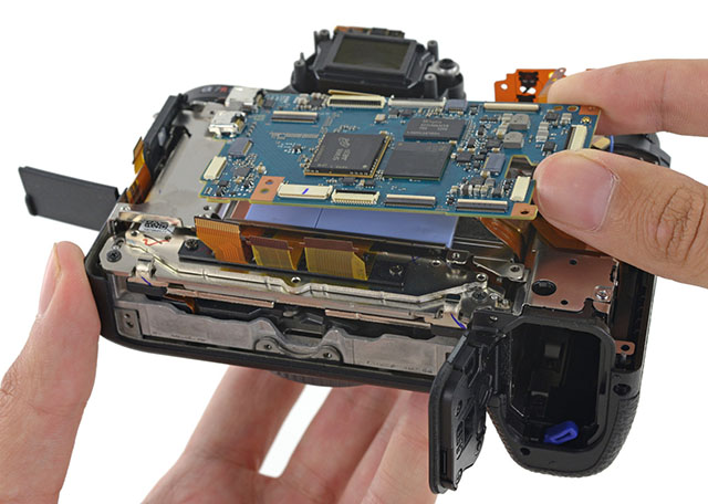
Chips for the camera’s wireless functionality. iFixit writes: “Funny how our smartphones are becoming more like cameras and our cameras are becoming more like smartphones, huh?”
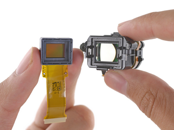
The 1.3 cm XGA OLED, which as 1024×768 pixels in half an inch — 2,560 ppi:
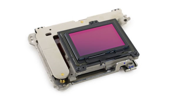
The 42.4 MP Exmor R CMOS back-illuminated sensor in its 5-axis in-body optical image stabilization cradle:
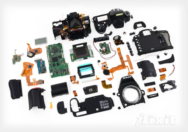
Finally, here’s what the Sony a7R II looks like when disassembled into its main components:
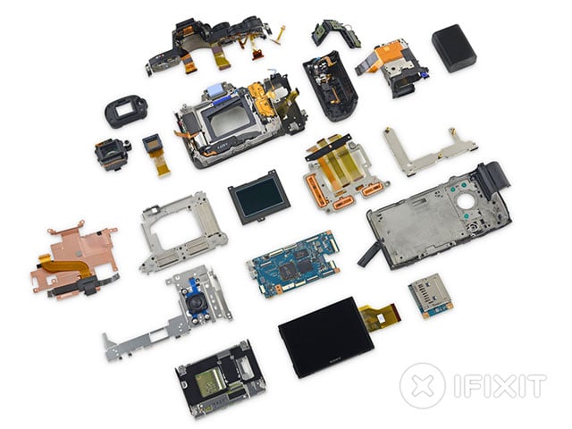
Overall, iFixit gives the Sony a7R II a “Repairability Score” of 4/10, with 10 being easiest to repair. While some surface level components (e.g. battery, tripod mount, viewfinder) can be easily removed and replaced, the internals are difficult to get to and the components are “intricately organized.”
You can find the full teardown and analysis over at iFixit.
Image credits: Photographs by iFixit and used with permission