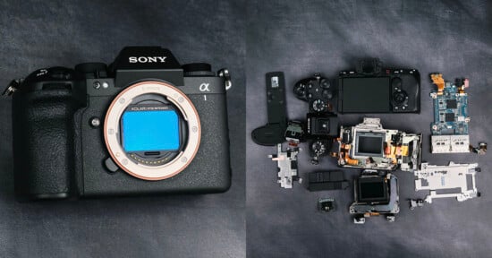
Sony Alpha 1 Teardown: The Inside of a Flagship Mirrorless Camera
The Sony flagship camera is here, the first of the mirrorless full-frame “holy trinity” of Sony, Canon, and Nikon to be released. Sony announced this beautiful beast back in January 2021, and today we’re going to take it apart, modify it into a full spectrum camera, and (hopefully) put it back together again.
Table of Contents
An Intro to the Sony Alpha 1
With 50-megapixel photos, 8K/30fps video, and the groundbreaking 30-frame-per-second burst mode, the Sony Alpha 1 really does it all. It’s the a7S III, a7R IV, and the a9 II all rolled into one. So naturally, it also costs about as much as any two of those cameras combined. It features a full-frame CMOS sensor, 9.44M-dot OLED electronic viewfinder, and has both electronic and mechanical shutters.
Sony has come a long way since the a7 was released back in 2013.
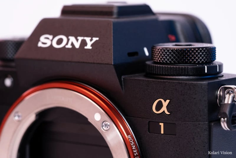
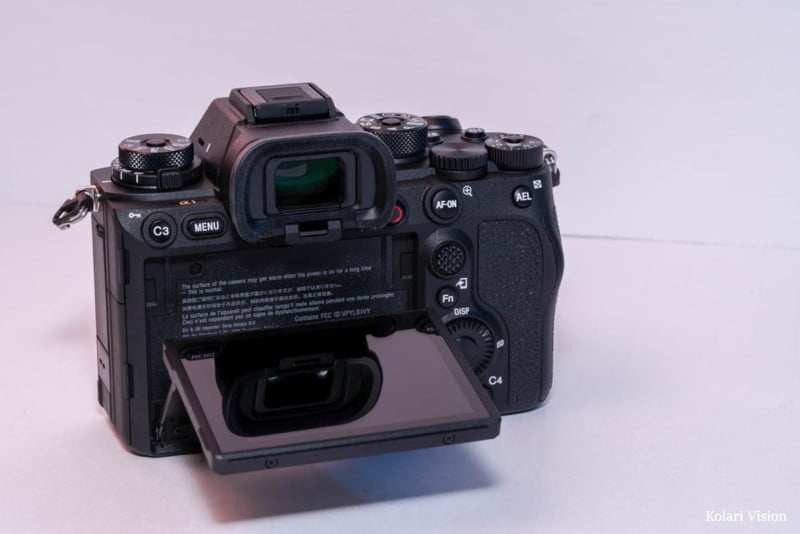
Let’s take a look at the outside first. The Alpha 1 is made in the familiar style of the a7 series, and features the beefed-up body and wider handgrip that Sony is using in its newest models, like the a7R IV. From the front, next to the focus assist light, we have the new visible light and IR sensor, which debuted on the a7S III. Sony promises that it will improve the camera’s white balancing capabilities (in artificial light). It’ll be interesting to see how well this works for the camera once we’ve converted it for infrared photography.
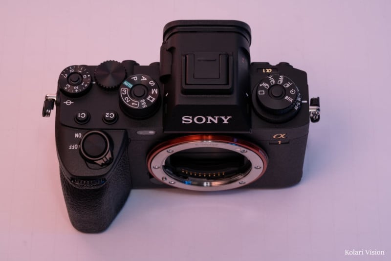
There’s a signature Alpha-model insignia designating this the Alpha 1, but for their flagship, Sony gave it a gold finish just like they did on the a9. Another shared feature with the a9 is the drive mode dial on its left shoulder, with the new HI+ burst setting. But what sets the Alpha 1 apart is the new focus mode dial.
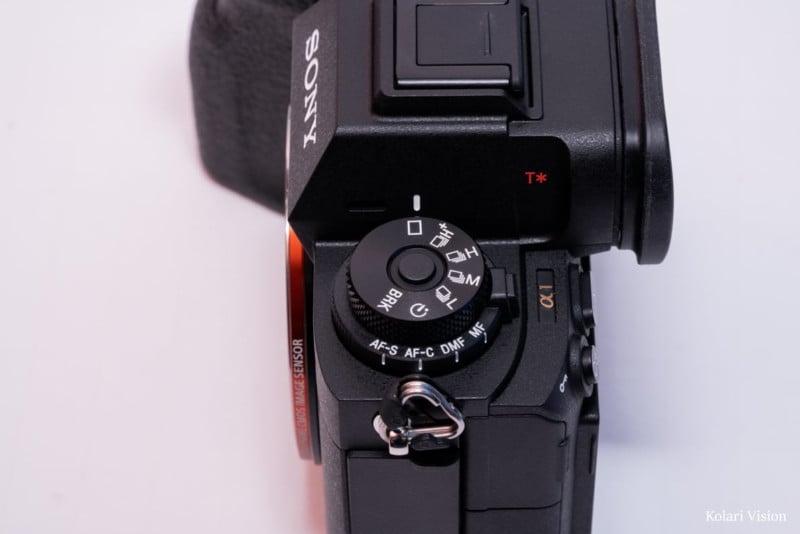
However, other than the new drive/focus mode dial, the top is completely identical to the a9 II, which itself wasn’t that different from the A9. Why fix what isn’t broken, I guess.
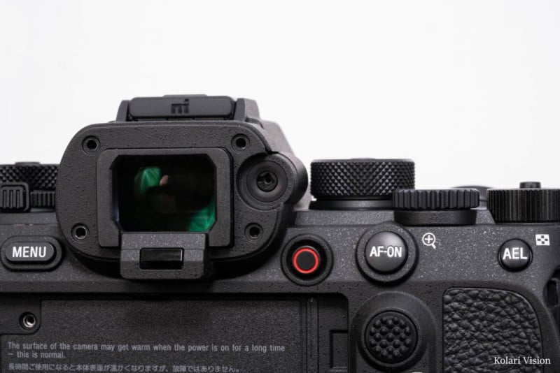
The back is more like the other Sony cameras of this generation. All of the buttons are rounded out and feel a lot clickier. The joystick is broader, textured, and runs smoothly. There are a couple of minor changes, such as the removal of the drive mode icon next to the dial, due to its relocation to the top. The video recording button has been changed from a red dot to a red circle, a small change but it’s a nice touch that makes it feel more prominent.
An interesting choice they made was giving this a tilt-screen rather than a flip-out fully articulating screen as they did with the a7C and a7S III, a decision that is sure to be a disappointment for some and a relief for others. I would’ve liked to have seen Sony attempt some kind of hybrid like the Nikon Z9 or Fujifilm X-T3, or that weird Pentax K-1 II (oh Pentax), but maybe they wanted to play it safe for this one.
Note: Another change on the Alpha 1 is that Sony switched from a metal build inside the mount to a plastic one, so unfortunately this camera isn’t compatible with our Kolari Magnetic Clip-in Filters for Sony E-Mount yet. Luckily, we’re working on creating a magnetic adapter plate to make our filters compatible with the Sony Alpha 1. Fortunately, other recent Sony cameras like the Sony a7 IV, a7R IV, a7S III are natively compatible!
Now let’s take it apart.
Opening Up the Camera
We’ll start by removing the screws on the bottom, and removing the plate and battery door.
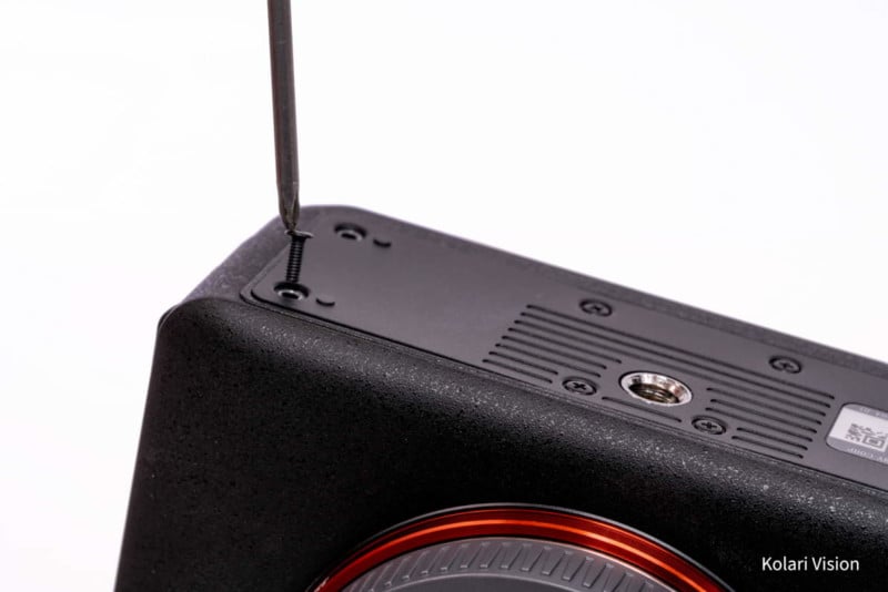
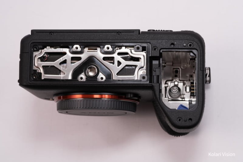
We see a very open bottom frame which should offer good cooling. This is the same one that we’ve seen in the a7R IV and a7S III, which was updated from the a7 III. The compartment fits the trusty Sony FZ100 batteries, which means if you’re upgrading from one of the recent a7 or a9 cameras you’ll be able to use the same batteries.
The battery is another thing that sets it apart from the other flagships. Sony elected to stick with a compact body over the built-in battery grip like the Z9 and R3, resulting in a lighter body that’s half the weight of the Z9. Personally, I’ve always preferred to prioritize ergonomics, and just keep a couple of spare batteries in my bag or pocket. Let us know in the comments which option you think is better.
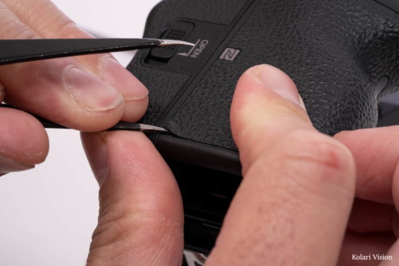
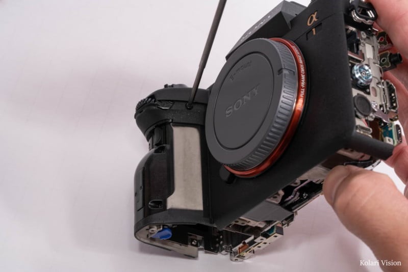
Next, we’ll need to peel off the leathers on the grip, which will give us a look at the NFC antenna.
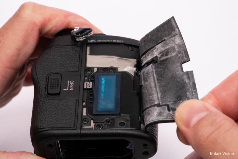
And remove the bottom frame.
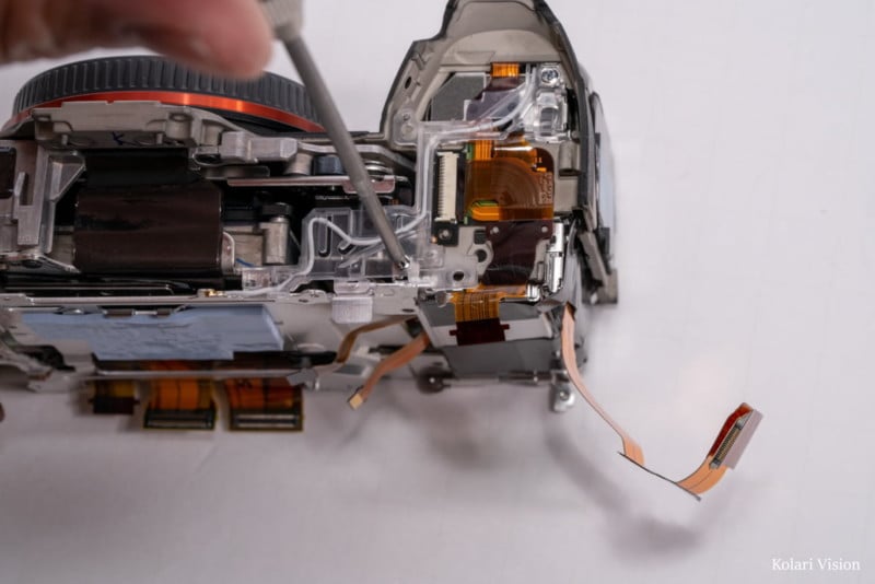
Then, we’ll remove the screws on the port panel. It looks like they apply Loctite on their screws to give it extra hold.
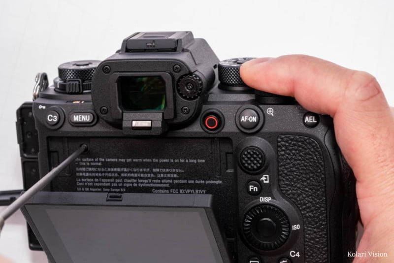
Then it’s just one screw on the back, four on the viewfinder, and one on the diopter.
Then we can take off the port panel, and lift up the back.
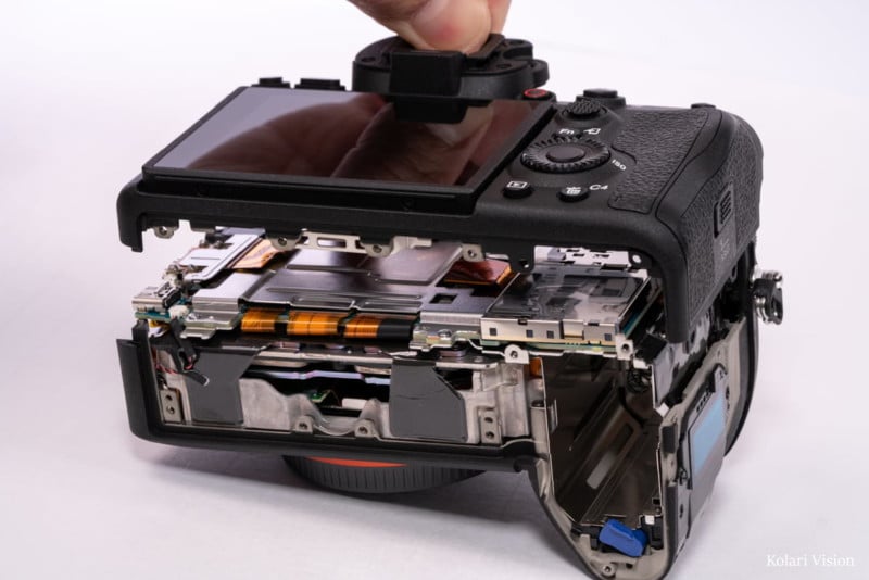
Looking closely at the edge, we can see that they’ve added some weather sealing material under the seam.
Now that we’ve popped the hood here let’s take a look.
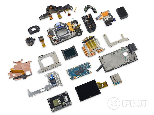
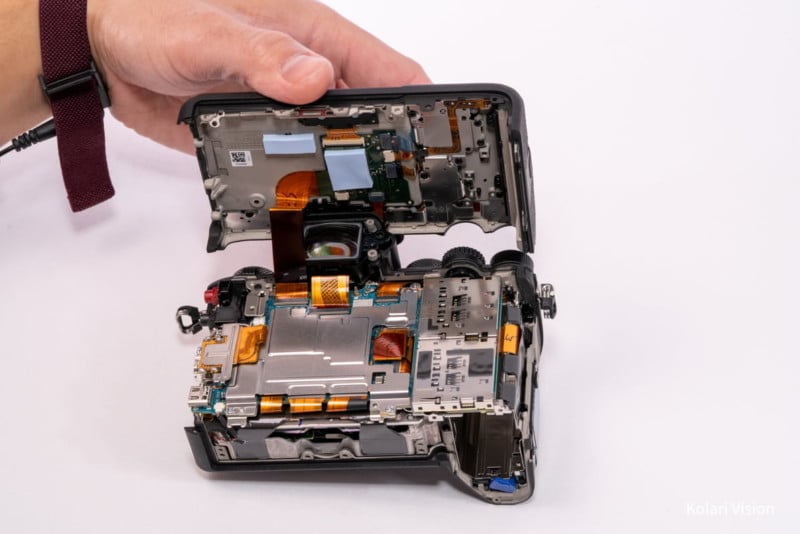
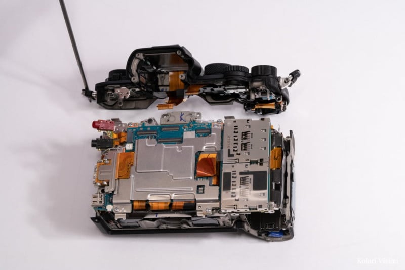
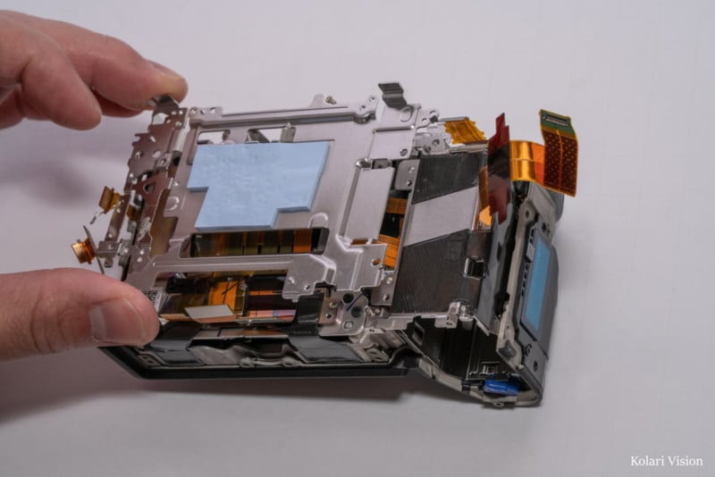
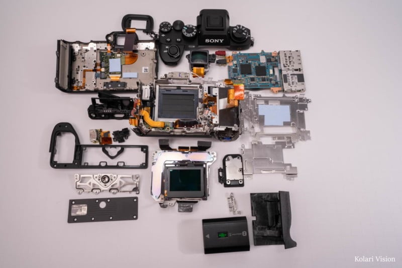
A Camera with Many Layers
There’s a lot to unpack here, literally, Sony cameras always have so many layers.
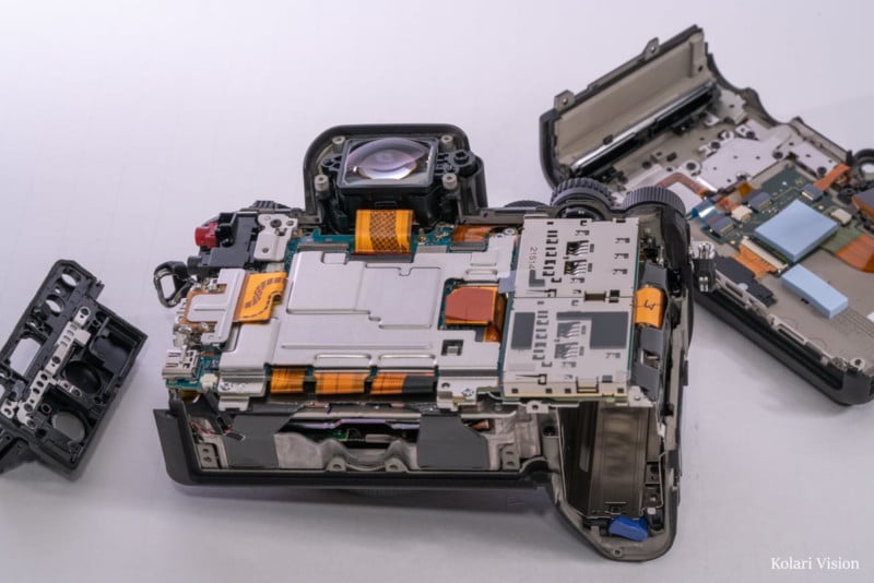
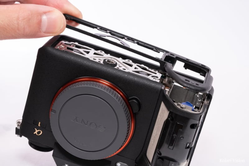
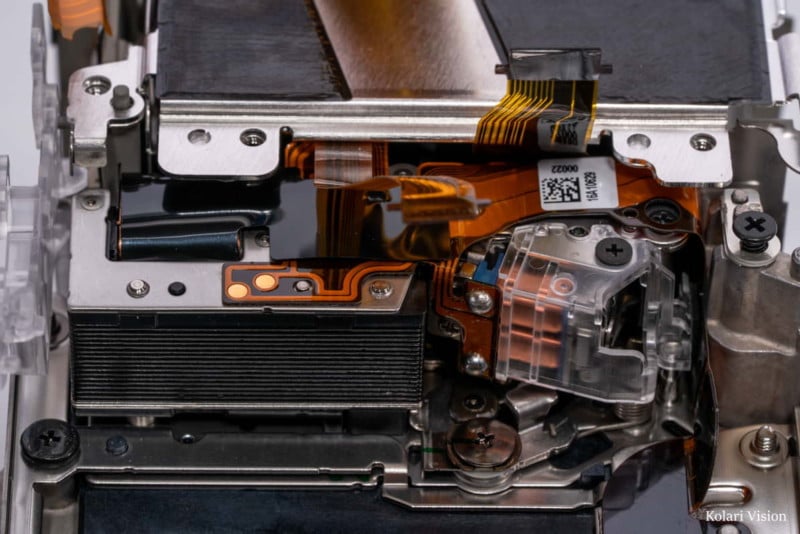
The metal thermal frame is the first thing that catches my eye. We’ve seen similar plates in the a7R II, but these were absent in the III, R III, and R IV. Now they added an updated version for the Alpha 1, as well as the a7S III. It’s no surprise that they needed to add more heat distribution considering performance those cameras are offering 4K 120FPS and 8K.
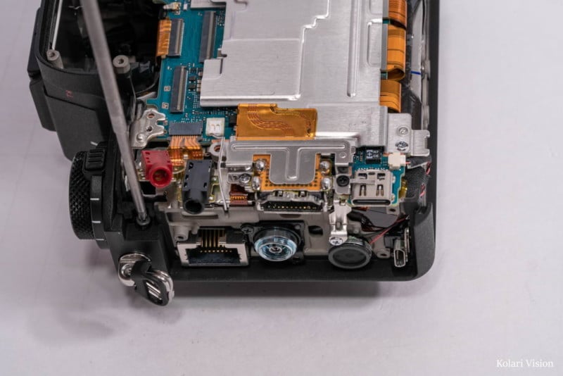
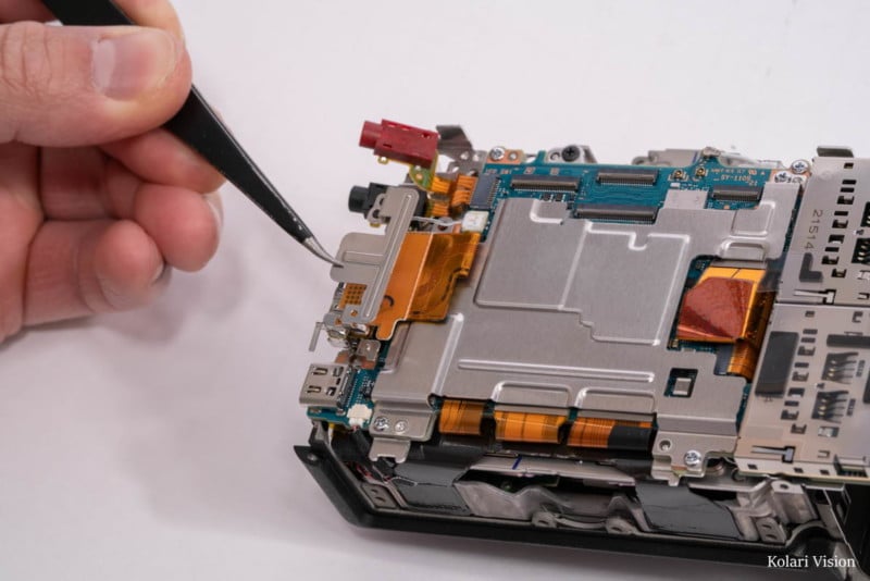
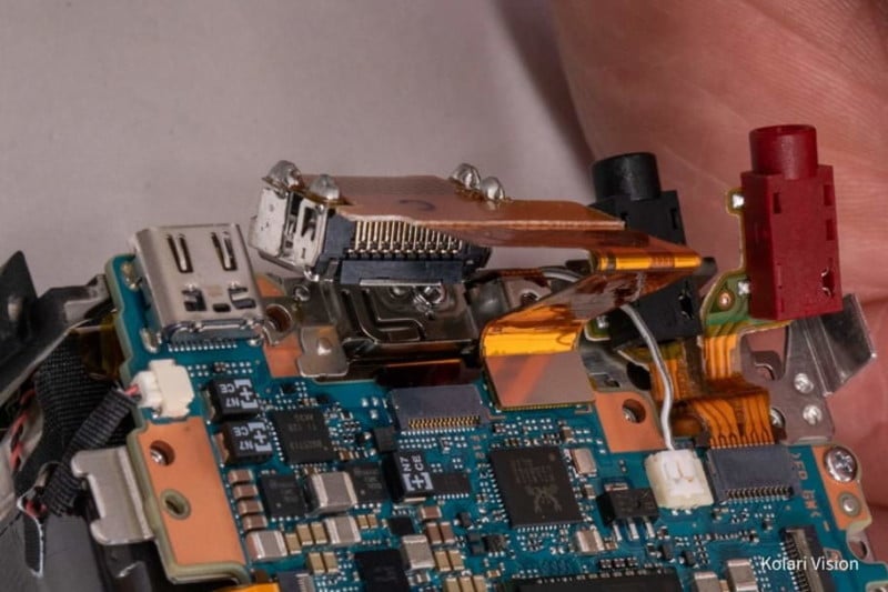
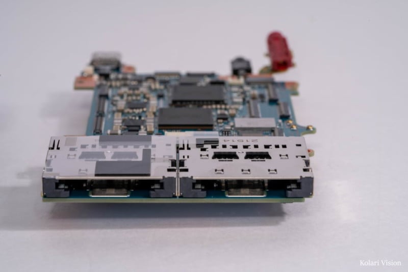
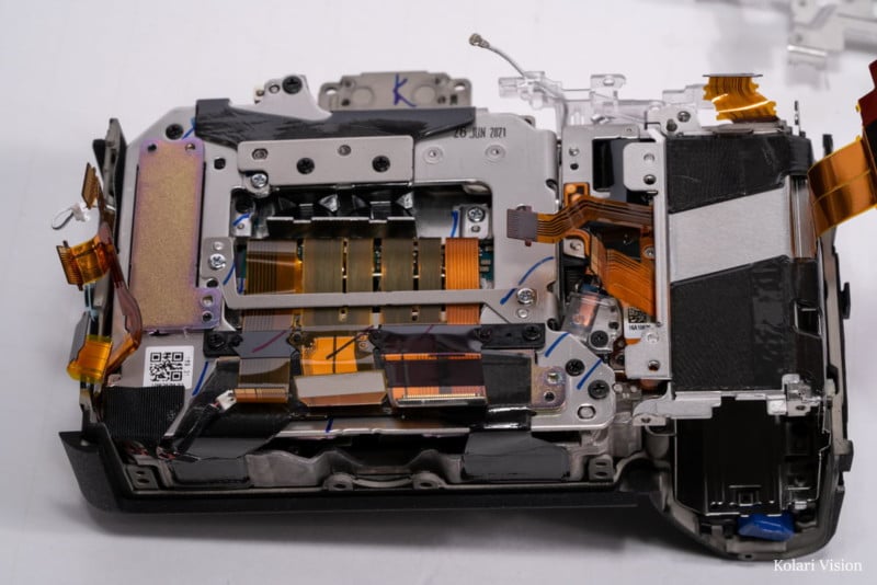
The overall layout is similar to what we’ve seen with other a7 cameras. Both card readers are mounted side-by-side on top of the board. What’s new and interesting is how the HDMI port is connected; where it used to be soldered onto the board, it is now connected by a folded flex cable and held in place with a bracket. That’ll make repairing or replacing that part much easier. We’ll take a closer look at that shortly, but first, let’s open it up a bit more.
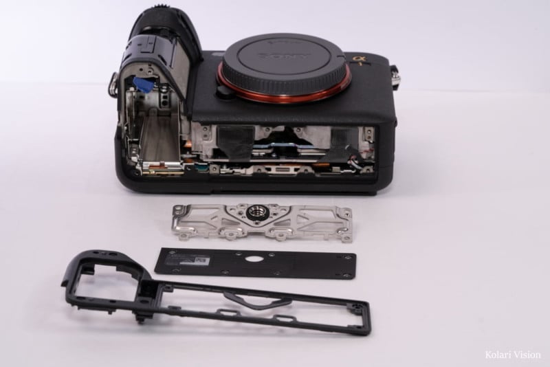
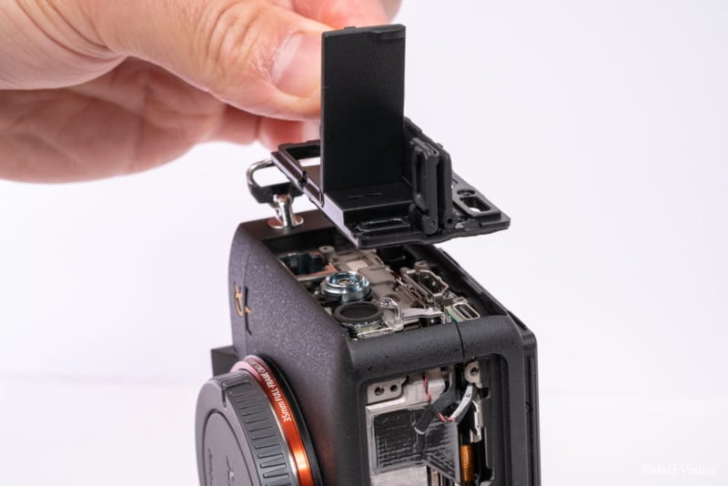
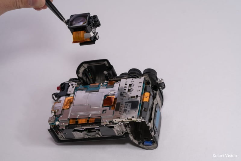
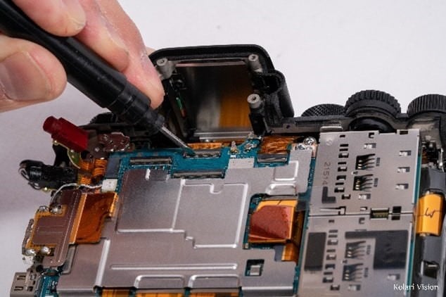
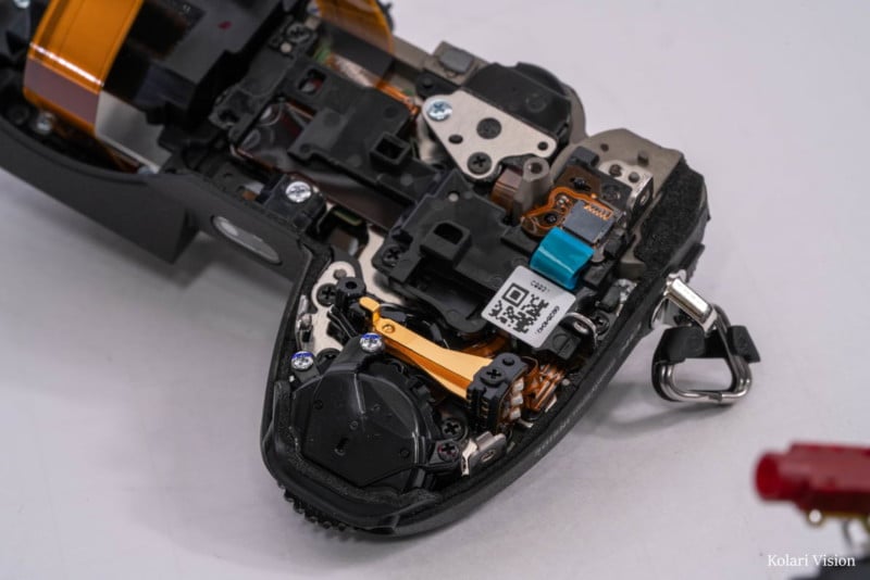
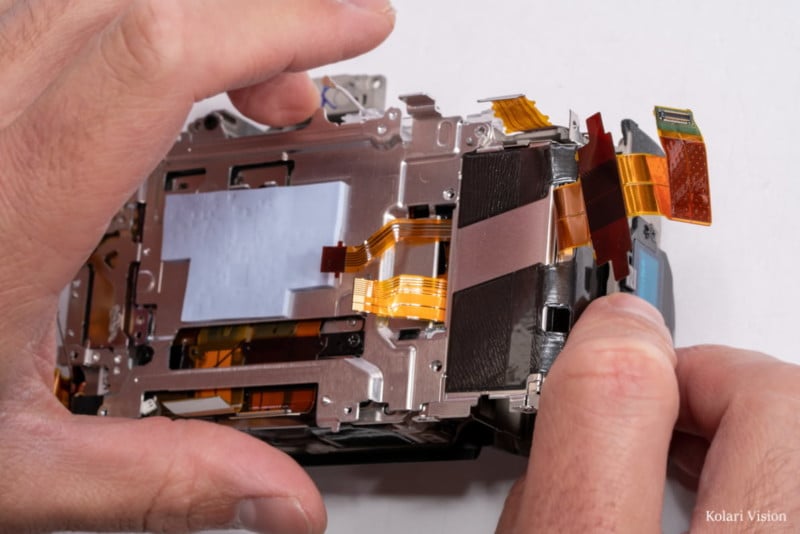
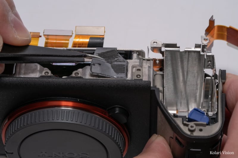
We’ll need to take out the viewfinder. In previous models the thermal pad behind the viewfinder would inadvertently adhere it to the back making it tricky to remove, however here they’ve added a plate that covers it.
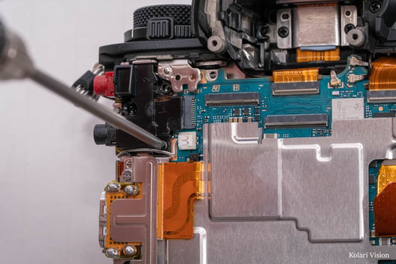
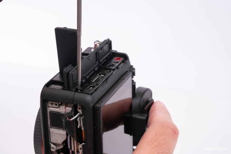
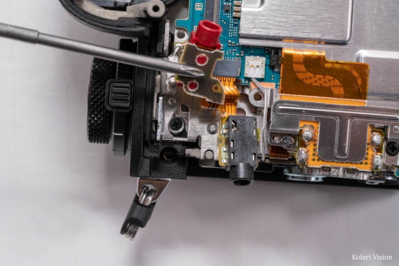
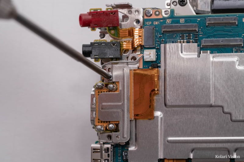
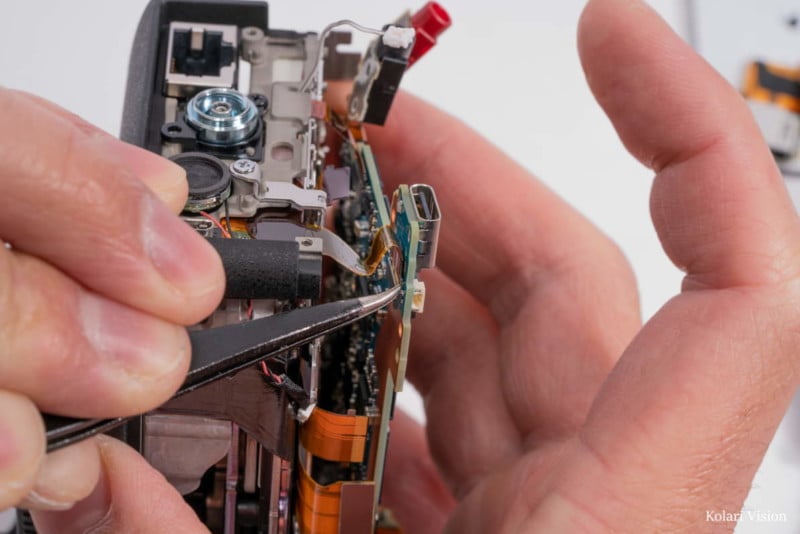
Then we take off the audio port brackets. Here we have a good look at the interior of the ports.
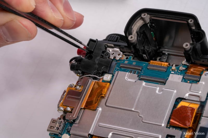
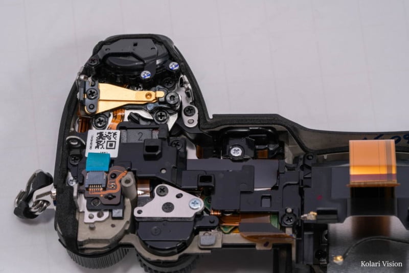
Next, we need to remove a few carefully concealed screws.
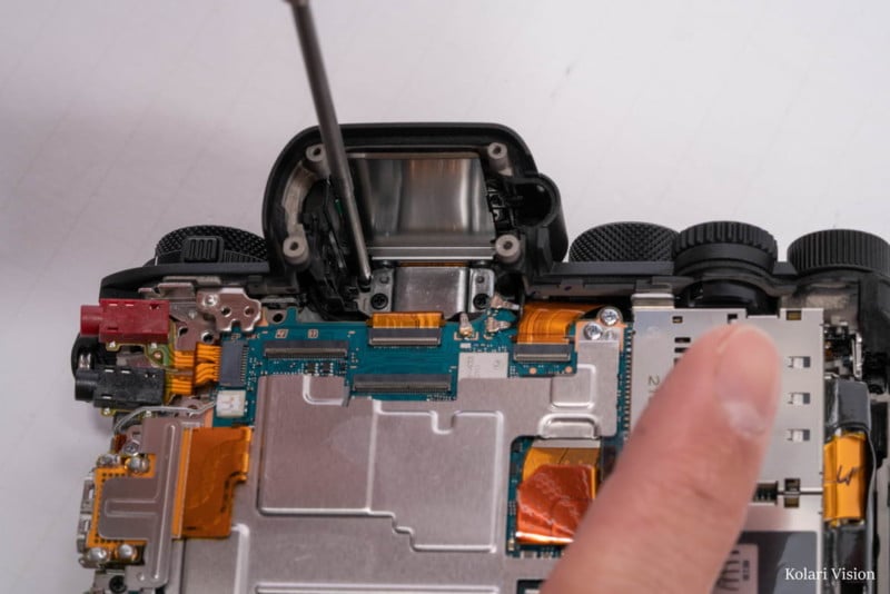
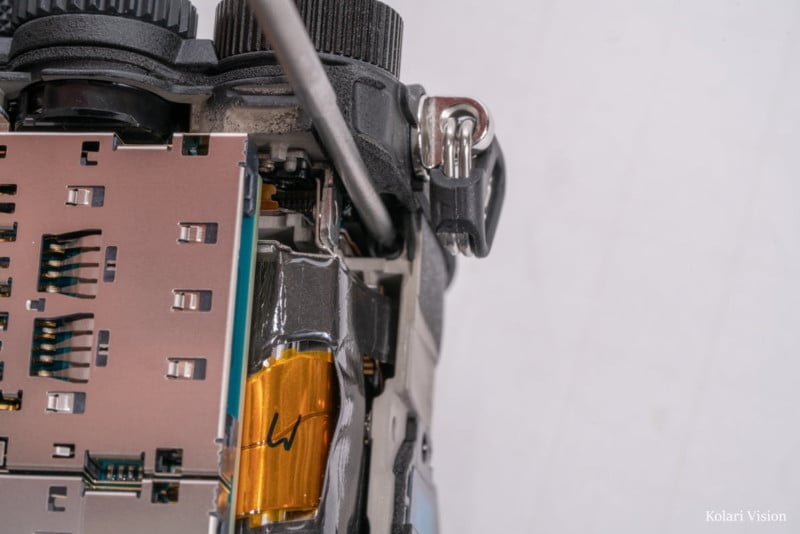
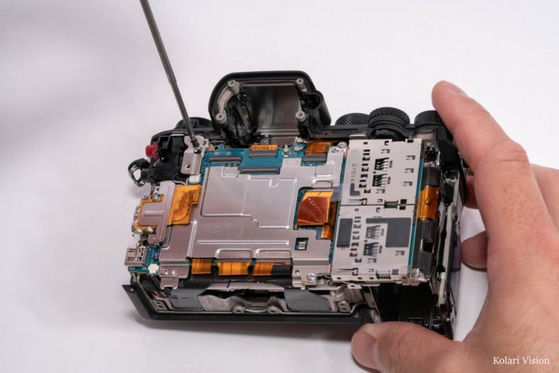
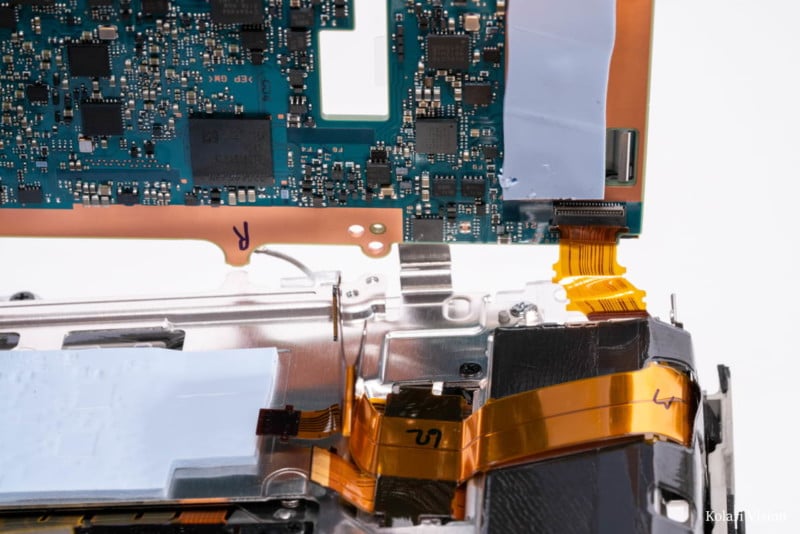
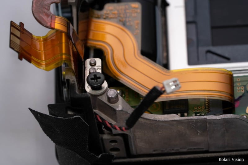
And remove the ribbon for the top. There are two new coaxial cables running up to the top, sitting alongside the antenna wire.
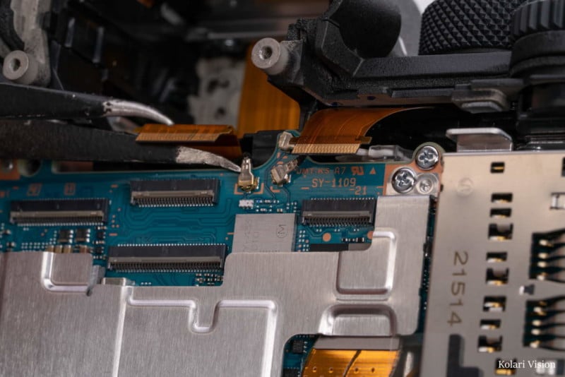
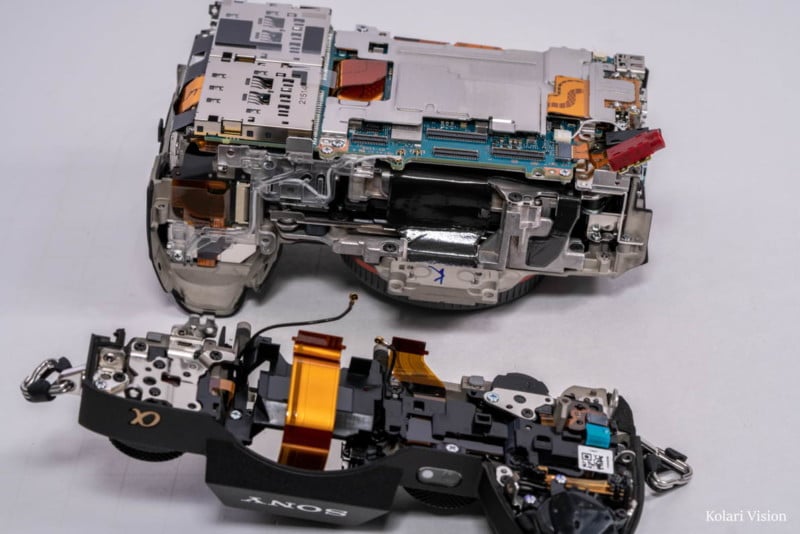
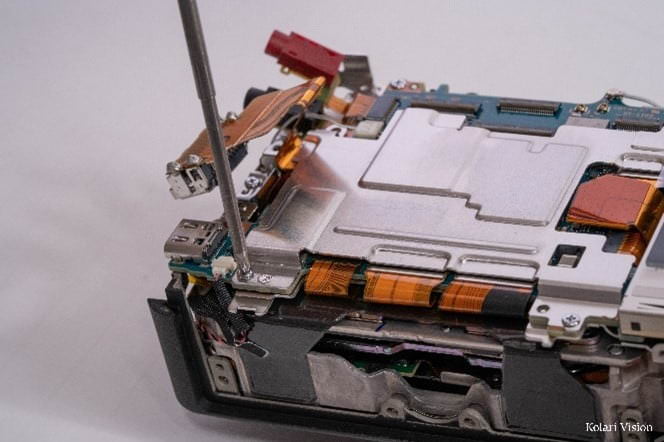
Now that everything is disconnected, let’s take off the top.
Looking along the edge of the top piece we can see more of the same weather sealing material.
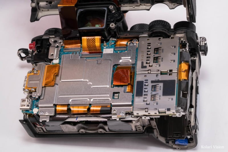
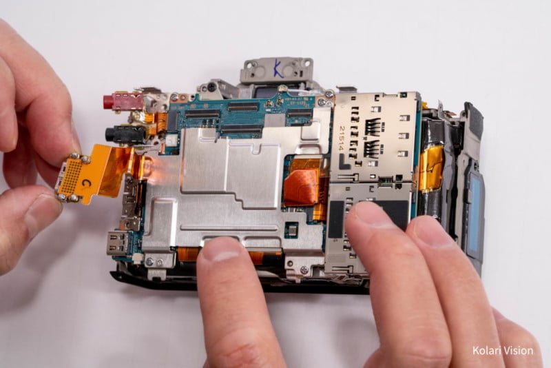
Now that that’s off, let’s take a look at that HDMI port connection. Once we remove the bracket holding it in place, it just hangs out. As you can see, the port block is just soldered onto the ribbon, which is connected to the board. That’ll make it super easy to replace.
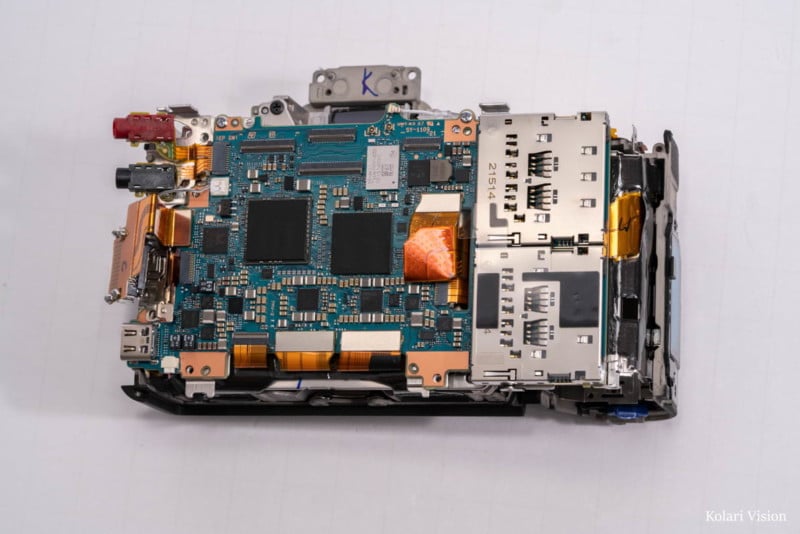
Let’s take the plate off so we can see the board.
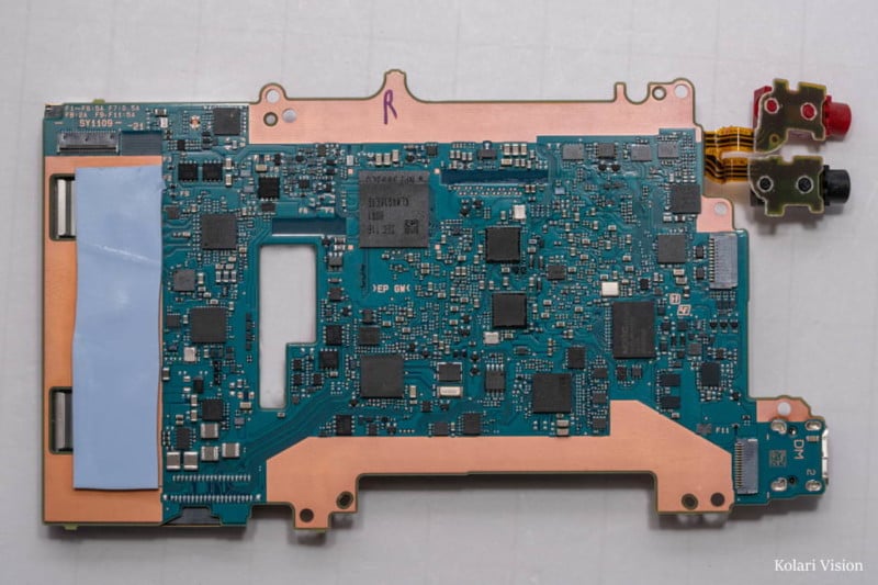
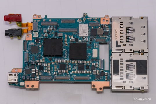
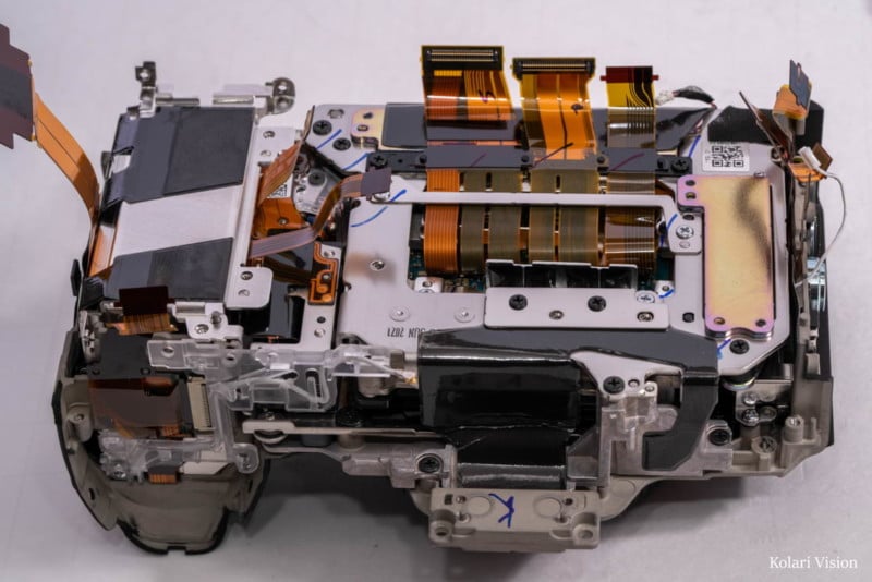
The Main Circuit Board
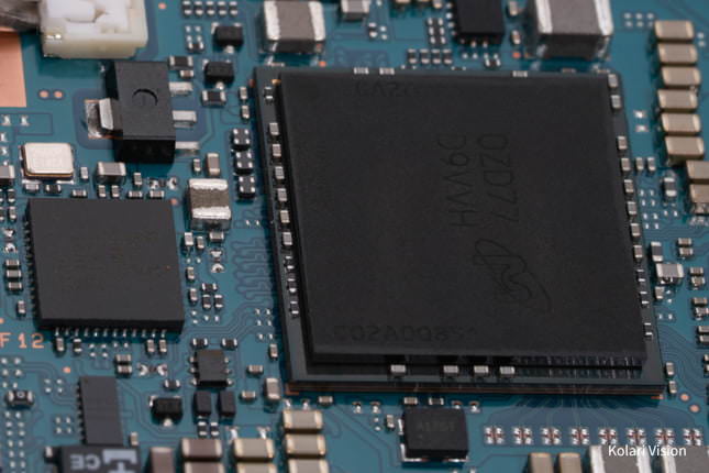
In the center, we see the brains of the operation, the dual Bionz XR processor.
Sony claims the processor is 8 times more powerful than the Bionz X processor, and it’d have to be to handle all the things this camera can do.
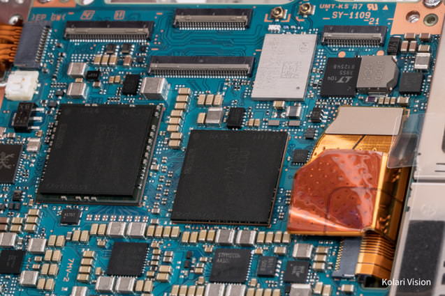
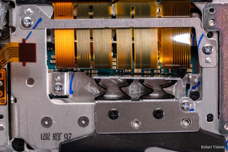
As always, there are a lot of ribbons on this. It’s interesting to see that two of the sensor ribbons have switched from clip-ins to press-on connectors. There are pros and cons to those, it makes it easier to remove but it can be tricky to put back on. That also means that it’d be easier to disconnect it accidentally, but if that happens you’re less likely to damage it than if you forcibly pull a flex cable out of its clip. The pins in general are less prone to damage and easier to repair.
Speaking of easy to accidentally damage, there are a couple of ribbons that connect to the underside of the board, such as the USB-C port connector. This is something we’ve seen in a lot of Sony cameras over the years. It’d be easy for an inexperienced tech to miss them, but fortunately, this is not our first rodeo.
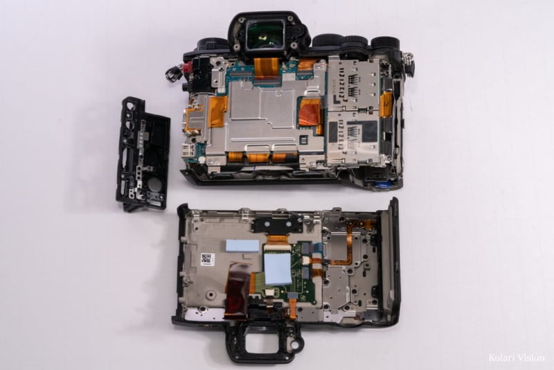
And with that, the board comes out.
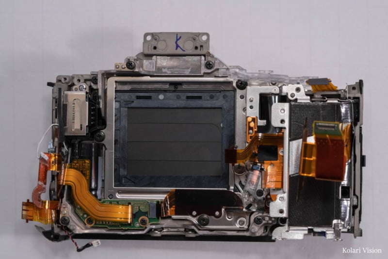
Beneath the board, is another layer of a metal heat sink. This one feels more condensed than what we’ve seen in other models.
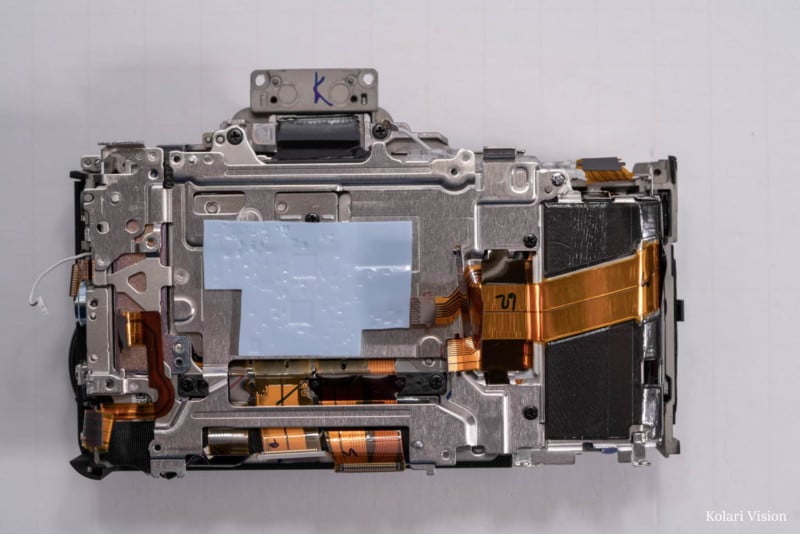
On the a7 III and a7R IV, it stretched over to the battery compartment, and the a7 III’s heatsink had ‘feet’ that extended down to attach to the front. Also, with the a7R IV they went with a more skeletal design, leaving gaps in the plate to cut down on the weight. Here, however, they have prioritized keeping it cool to keep up with the performance demands. They’ve included a layer of heat pads in the middle. Unfortunately, it doesn’t seem to have been as effective as they’d hoped, as we have heard some complaints of overheating, although nothing as bad as with the Canon R5.
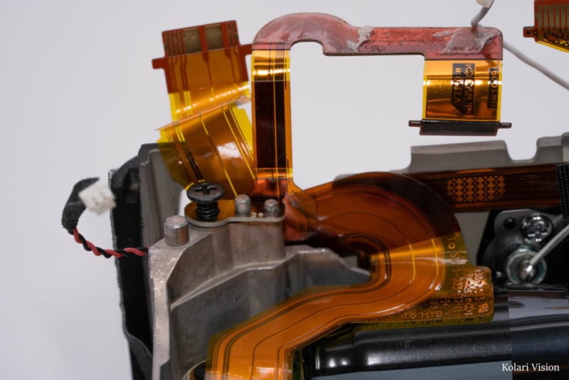
Another nice little update is the wings on the NFC flex cable that hook into the heat plate and hold it in place. It’s always hard trying to wrangle the different ribbons in place around the board, so this will make reassembly a bit easier.
They’ve also added a clear casing around the coaxial cable at the top which should offer some extra protection.
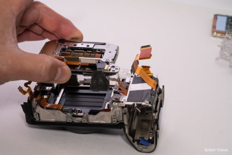
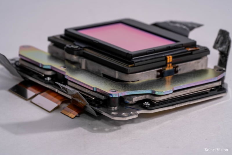
We take the plate off and there we have the sensor.
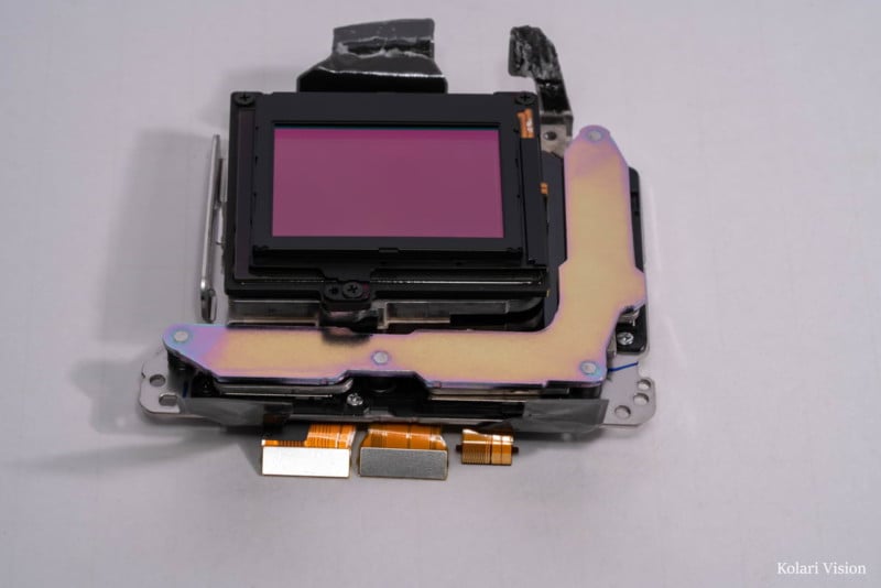
Revealing the Image Sensor
Surrounding this beautiful piece of engineering are a few strips of heat tape, for additional temperature control. Once we peel that back and remove the screws, we can remove the sensor.
We’ve recently learned that the sensor this camera is using is the IMX610, which is a brand-new sensor that Sony developed exclusively for the Alpha 1. Here it is, in all its glory.
The Alpha 1 may look identical to its predecessors, but there are a lot of little changes inside and out that make this a very impressive camera.
That’s it for this lengthy teardown of the Sony Alpha 1 mirrorless camera. We hope it was interesting and informative for you. Thanks for reading!
About the author: Alex Mirchuk is a technician at Kolari Vision, which offers infrared conversion and other modifications and products for digital cameras. The teardown was performed by lead technician Jared Barcelona. Find out more at the Kolari Vision website. This article was also published here.