Why and How Fuji Cameras Produce a Strange Purple Flare/Grid Artifact
When FujiFilm’s X-Trans III sensor was introduced in the X-Pro2, many users began noticing a strange new artifact in their backlit photographs. Upon further experimentation, it became apparent that the same artifact could also be found in images from cameras using the older X-Trans II sensor.
Many theories have been bandied about in internet photography forums, pointing the finger at specific lenses, certain body production batches, and, sadly but predictably, the users who dared to suggest there could be flaws in the output of a rather expensive camera, but very little information of a technical kind has been published on the problem.
In the third episode of our X-Trans saga (the first was about color detail in the in-camera JPEGs, and the second about luminance detail in RAW processing), I will share some of what I’ve uncovered about the nature of this particular artifact on my reluctant (some might say heroic) journey to become an expert in FujiFilm’s quirky and eccentric sensor technology. Come Sancho, we must slay this wizard who enchants the people’s sensors!

Joking aside, the first thing I’ve discovered about this issue is that it is very rarely encountered in practice by those who abstain from shooting facing into the sun or similar light sources. For those who indulge in flare-filled portraits or landscapes with the sun in the frame, however, it may be a more frequent occurrence.
Let me be perfectly clear: I’m not trying to play-up the severity of this problem by writing this article (it’s only happened to me a few times), only to offer some insight into how and why it happens, sharing what I have learned from many hours spent studying the issue in detail.
Bear in mind that this is a highly technical subject and this article will only scratch the surface of the issue. If you’re expecting a discussion on semiconductor fabrication techniques, electron beam coatings, etc. you’ll have to look elsewhere. The information presented here comes entirely from my own original eye-straining analysis of real-world images.
I’m not claiming it to be 100% accurate. What I call “left” could be “right” etc.—there appear to be no authoritative reference materials published on the matter by FujiFilm or anyone else. (If someone out there reads Japanese and knows where to find the patents, by all means send them my way.)
The nature of the grid
This artifact is particularly interesting because it allows the layout of the X-Trans CFA to shine through, as it were, in the demosaicked image—something which should never happen. (If you look closely you can make out the “X” of X-Trans: uninterrupted diagonal lines of green pixels which criss-cross the sensor.) Not even the camera JPEG output, generated with FujiFilm’s supposedly expert proprietary image processing, is immune to this problem (And, yes, I’ve confirmed that Iridient isn’t immune to it either.)
Due to the complexity of X-Trans processing, the appearance of the effect will vary with the particulars of the demosaicking algorithm in use, but no algorithm will be completely immune from its effects. It may be possible to include special measures to mitigate this artifact in a new algorithm, but this would further increase the complexity and computational load, and come at the cost of resolution and the introduction of new types of artifacts.
Why is there a grid?
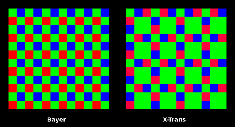
First and foremost, the reason that this effect is apparent at all is because the of the particular arrangement of the X-Trans CFA, with larger gaps between same-colored pixels. If a sensor utilizing a Bayer CFA were similarly affected, the presentation would probably be more like speckling than a grid, and certainly wouldn’t show any X’s, and could more effectively be removed by traditional noise reduction techniques.
What causes the grid to appear?
The X-Trans II sensor found in the X-T1 (but introduced earlier in the X20, X100S, and X-E2) was the first to bring on-sensor phase-detect autofocus technology to FujiFilm’s X series of cameras. X-Trans III, found in the X-Pro2, X-T2, X-20, and X100F, extends this concept with a larger coverage area and more phase detect pixels (PDPs).
FujiFilm’s technology adds an additional layer to the sensor, a masking layer between CFA and the photodiodes. This mask is only apparent in the central region of the sensor (the extent being greater in X-Trans III than X-Trans II).
It should be noted that there are many more masked PDPs on the sensor than there are “AF points.” 2.8% of pixels in the PDAF area of the sensor are masked. On the X-Trans III sensor, the PDAF area is 3000×3000 pixels (9MP), containing a total of 250,000 PDPs. AF points in this context are a software construct—the values of many PDPs are be used to determine the focus at a single AF point.
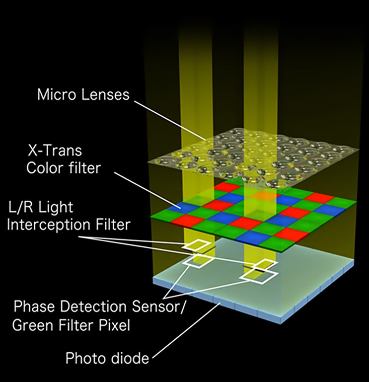
What this masking layer does is block half of the masked pixels from receiving light from the “left” side of the image, the other half from receiving light from the “right” side of the image. When the image at the AF point is in focus, the light from the two sides coincides (is in phase). Each PDP is only receiving up to half the amount of light of an unmasked pixel (1-stop less in photographic terms).
This can be compensated for by doubling its brightness in software, with the penalty of also amplifying its noise. This system is also subject to interaction between medium to high frequency detail in the image and the mask (particularly apparent in feathers and fur), but that’s another problem for another day.
This particular implementation of on sensor phase detect is of the “horizontal” type, meaning it is only sensitive to vertical edges in the subject. Most DSLR cameras, in contrast, have AF modules which include a mix of horizontal, vertical, and, more recently, cross-type sensors. Being limited to horizontal only sensing is a limitation of all currently deployed on-sensor PDAF technologies that I’ve surveyed, and isn’t exclusive to FujiFilm.
But what does any of this have to do with the grid artifact?
There are at two main factors in play, both of which seem to involve this pixel masking layer. The overall effect is a combination of these factors, the precise appearance of which depends on the particular angle/orientation of the flare and the region of the frame the flare covers.
The phase detect pixel effect
To put it simply, it is possible for extraneous light to pass through the lens and strike the sensor in such a way that most of the “left” (or “right”) masked PDPs are not illuminated (although everything else is).
Don’t believe me? Forget about optical inversion for the purposes of this thought experiment (it’s a superfluous complication): Say that a cone of hard light (flare) is shining on the sensor from the “right” direction. This illuminates all of the unmasked pixels, and all of the “right” masked pixels, but none (or few) of the “left” masked pixels. It really is that simple.

When a demosaicking algorithm, even FujiFilm’s proprietary one, attempts to construct a full color image, these shadowed pixels misguide the interpolation, spreading the error out over a wider area, and allowing the pattern of the CFA to show through. Because of the alternating pattern of “left” and “right” PDPs horizontally across the image and the 12×12 repetition of the PDP mask, this effect creates an artifact with a period of 6 pixels horizontally and 12 pixels vertically across central region of the image.
OK, but why is the flare purple?
If you’ve been paying close attention (particularly to the diagram above), you may have already figured that out: the flare isn’t purple, it’s anti-green. Purple, more specifically magenta, is the color you get in RGB additive color mixing when you subtract green from white. That is to say, a mixture of just red and blue.
The flare appears purple or magenta because of all the thousands of masked off pixels on the X-Trans II/III sensor, every single one of them is a pixel sensitive to green light, and located in exact the same place in the CFA pattern (upper right hand corner of that block of four green pixels). When a (white) veiling flare illuminates all of the pixels except for either the “left” or “right” PDPs, this leaves a deficit of green signal.
Note: in the real world, flares do tend to have a color tint of their own, but that doesn’t change the principle at work.
The masking layer thickness effect
The PDP influenced part of the effect only appears in the central region of the sensor where the masked PDPs are, but the purple flare/grid artifact affects the entire sensor. This effect seems to be caused by the added thickness of the masking layer or perhaps some other property of the sensor’s optical stack.
What appears to be happening in this effect is that light is striking the sensor from the “up” direction and casting a “shadow” from one row of pixels to the row below. This is presumably happening in the gap created by the masking layer, between the CFA layer and the photodiode layer.
Pardon the annoying animated GIF below, but this was the easiest way to visualize what’s going on. This animation comprises three frames: The first frame is the (naturally) monochrome RAW sensor data, the next frame is the raw sensor data with each pixel colorized to match the X-Trans CFA pattern, the final frame is the demosaicked image data (where the grid and purple color can be seen.)
This is from an area of the image which would have been uniformly dark (shadow) were it not for the flare.
As you watch this animation, pay particular attention to the top two pixels in each 2×2 block of green pixels. In the row below, you can see the intensity level that those pixels should have, notice how they’re darker, and that the green pixel below a red pixel is a different shade than the green pixel below a blue pixel? Can you also see that all the blue pixels immediately below a red pixel are darker than the blue pixels below a green pixel and vice-versa?
The green pixels don’t appear to cast any kind of “shadow” in this way, only the red and blue pixels do. Perhaps because the green filter is weaker or because of color shifts caused by the various coating involved or some other effect—the physical particulars don’t really matter at this level of analysis.
This pattern affects every 3×3 group of the X-Trans pattern, and repeats on a 3 pixel period horizontally and vertically across the image, creating the bulk of the “grid.”
OK, but why is this one purple?
It should be obvious from referring to the figure illustrating the X-Trans CFA that every third row of X-Trans has an equal number of red, blue, and green pixels. That is to say, it is 33% green. The remainder of the rows are 66% green.
When a 33% row casts its “shadow” on the 66% green row below it, it is removing a significant amount of green signal from the image (the image of the flare, that is) simply because the 66% green rows have a larger contribution to the green channel. This isn’t even accounting for the fact that none of the green pixels appear to cast this “shadow.” This minus-green effect results in the flare appearing magenta overall.
All told, this “shadowing” effect is responsible for the majority of the magenta tint.
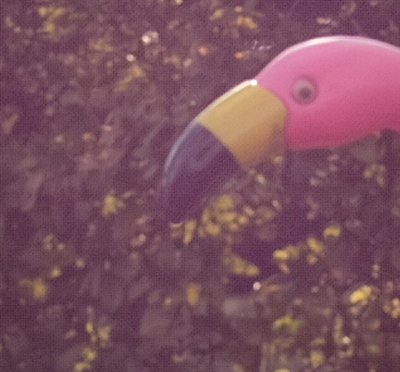
Examples
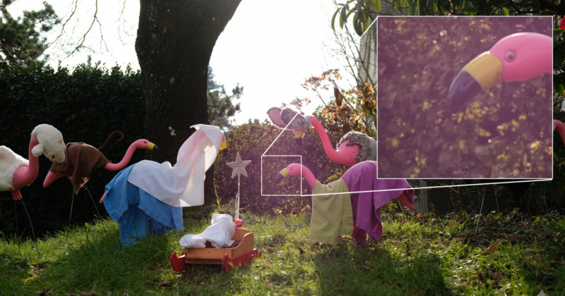
Well, since you’ve read this far, I guess I’d better show you some examples. Unfortunately, Sancho and I were unable find any conveniently located windmills (trust me, there are at least a couple of dozen people on the planet who will find this joke mildly amusing), so this plastic flamingo lawn nativity scene will have to do.
Side Note: Below is an artist’s depiction of person who criticizes the artistic merit of example images in articles about camera artifacts:

You may think that the example image below isn’t a good one. Please try to bear in mind that the purpose of the example is to show the purple flare/grid artifact in a real-world context, not to present a composition for artistic criticism.
You may be tempted to point out that the image is out of focus, and think that this somehow invalidates the example. It does not. Indeed, it may very well be out of focus, and if you’ve been following closely you will know why: flare (and to some extent any backlighting) causes the on-sensor phase-detect autofocus system of these cameras to go haywire. The camera doesn’t know what’s in focus. It’s hopeless. I suspect that in-focus examples of this problem are the exception rather than the rule.
The image below was shot with the FujiFilm X-T2 using the Fujinon 35mm f/2 lens at f/4.0 and ISO 200.

What can be done about it?
Unfortunately, not much. From a software perspective, you could insert some preprocessing before the demosaicking algorithm to identify the flare area, add some of the value of the red/blue pixels to the green pixels in the rows immediately below them (assuming the flare usually comes from the “up” direction), thus compensating for the masking shadow.
In addition, you could have a demosaicking algorithm that ignores all of the PDPs, interpolating around them. That would probably get rid of the grid for the most part, and the purple aspect, but doing so would come at a cost to resolution, in particular the green/luminance resolution, an extra quantity of which was supposed to be the saving grace of the X-Trans CFA. This would all be absurdly complicated for a demosaicking algorithm and likely to introduce some new artifacts.
A hardware solution would be to ditch the current method of on-sensor PDAF in favor of something more sophisticated like Canon’s Dual Pixel AF technology (with which such imbalances as described herein are presumably impossible because there is no masking layer and no lost light). No camera or lens yet designed can perfectly reject flare; this problem is less about the flare occurring, which is inevitable under the described conditions, and more about the way the sensor responds to the flare.
It’s worth pointing out that all of these problems could have been anticipated by FujiFilm’s engineers before ever coming close to the manufacturing stage—they just didn’t think it was a big deal. Given that they went on to release three more camera models with the same sensor design after the problem was discovered by the public, I wouldn’t hold my breath waiting for them to issue a recall over it.
Conclusions
It is obvious from the single-pixel extent of the artifact in the raw sensor data that this is a sensor-level effect. The grid/purple flare is not due to internal reflections between the sensor and the lens (although this kind of reflection certainly can and does happen with mirrorless cameras), but to optical or electrical effects occurring within the sensor package itself.
Any precautions to avoid or eliminate flare may reduce the the symptoms, but the disease remains. The underlying problem is exacerbated by presence of the X-Trans CFA, which imparts both the grid-like luminance effect, and the majority of the magenta colored chrominance effect.
As can be plainly seen, the overall effect isn’t particularly noticeable at typical (at the time of writing) Web display resolutions. The purple tint is present at all display sizes, whereas the grid requires magnifications higher than about 25% to become apparent. However, the grid, consisting of high frequency detail, is subject to enhancement by sharpening and other post-processing steps, which may increase its visibility at lower resolutions.
Whether or not you consider an image with this artifact to be completely ruined is entirely up to you—many people consider an image with any degree of flare to be ruined—but this is definitely a lower level of fidelity than I’m accustomed to seeing in similar situations. Furthermore, as already mentioned, due to the mechanisms involved, it is likely that the grid artifact and phase detect AF failure are, shall we say, comorbid and linked.
This artifact is characteristic of the FujiFilm X-Trans II/III sensor, allowing affected images to be easily be identified. I can’t recall another instance of such a complex and distinctive artifact. It is, however, easily avoided by abstaining from photographing backlit subjects.
Is this mere tilting at windmills? I don’t believe so. The problem is real, if infrequently encountered, and having an understanding of its nature can help us avoid it.
About the author: Jonathan Moore Liles is a photographer, writer, musician, and software architect living in Portland, Oregon. The opinions in this article are solely those of the author. You can find more of Jonathan’s work on his website, Instagram, and Bandcamp. This post was also published here.