Samsung’s ‘Nanoprism’ Sensor Technology Promises Brighter, Clearer Photos

Samsung, Google, and Apple are in a three-way battle when it comes to photography, but of the three, Samsung is typically the most forthcoming with explaining new advancements in its sensor tech. It recently published a deep dive into its nanoprism technology, a new type of microlens that it says improves light gathering significantly.
Oversimplified, the more light a sensor can gather, the better the photos. This basic principle becomes more difficult as sensors and pixels get smaller. On smartphones, where sensors are incredibly small compared to standalone cameras, getting light to pixels is a challenge.
“Technology has evolved in the direction of making pixels smaller and smaller to realize high-resolution images without increasing the size of smartphone camera modules. However, this has gradually reduced the sensitivity of unit pixels and caused image quality degradation due to crosstalk between pixels. As a result, it was hard to avoid the limitation of a sharp decline in image quality in low-light environments,” Samsung says in a post to its blog, seen by Image Sensors World.
All smartphone makers have chosen to deal with the problem of poor low-light photos in different ways, with software and algorithms being the most popular approach — even for Samsung. But the company is implementing a concept first proposed back in 2017: nanoprisms.
Each pixel on a sensor is accompanied by a microlens that focuses the light onto the pixel. The better the microlens, the better the light gathering capability of each pixel, and therefore the better quality the final image. Larger pixels are easier to build microlenses for, but as the pixel gets smaller, microlenses get more and more difficult to create and control.
“In the existing microlens-based optics, the microlens and the color filter of the pixel are matched 1:1, so only the light of the color corresponding to the color filter of each pixel can be accepted by the pixel. In other words, there was a physical limit that light could only be received as much as the size of the defined pixel,” Samsung explains.

Nanoprism technology changes the design of those microlenses so that instead of a standard rounded lens, the pixel is accompanied by a nanoscale structure in the microlens position, which directs light to each color-matched pixel.
“Simply put, the amount of light received by each pixel has increased, because light that was lost due to color mismatch can be sent to adjacent pixels using refraction and dispersion of light.”
Replacing a microlens with a nanoprism allows pixels to receive more light. Samsung argues this is a far better solution than the current method, but if that is the case, why has it taken eight years to implement?
“Commercializing Meta-Photonics technology in image sensors was a challenging task,” Samsung explains. “As can be inferred from its name Nanoprism, it was especially difficult from process development to mass production because precise and complex nanometer (nm) structures had to be implemented in pixels. In order to bring the new technology to life, special techniques and methods were introduced, including CMP (Chemical Mechanical Polishing) and low-temperature processes for Nanoprism implementation as well as TDMS (Thermal Desorption Mass Spectrometry) for image sensor production.”

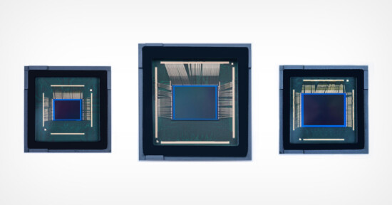
The commercial implementation of the nanoprism technology is called Isocell JNP, which went into mass production this year and is already incorporated into “recent smartphones.” Samsung did not say what smartphones or which camera systems Isocell JNP can be found in, but does say that where it is used, there is a 25% increase in sensitivity compared to previous sensors of the same type, with the same specifications, but using the prior microlens technology.
Image credits: Samsung Semiconductor