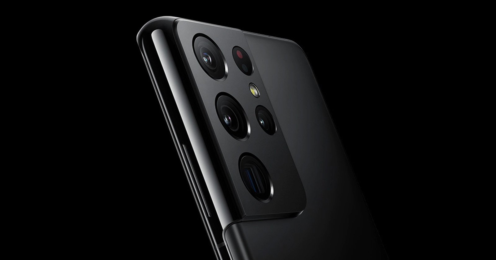
New Lens Tech Poised to Eliminate the Smartphone ‘Camera Bump’
Metalenz, a startup that has just emerged from “stealth mode” today, has revealed its vision for the future of smartphone lenses, a segment of the market that has not seen much change in the last ten plus years.
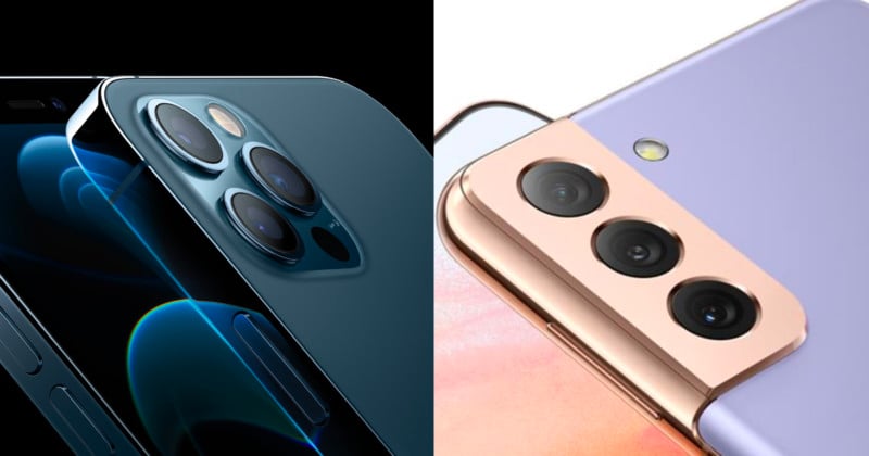
While sensor technology continues to see notable changes and improvements over time, the technology of lenses has remained rather stagnant, and fundamentally unchanged since the iPhone launched in 2007.
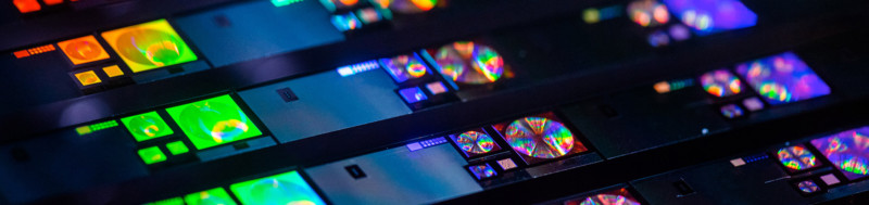
Metalenz wants to change that with a “flat lens system” that it says utilizes a new technology called optical metasurfaces. The claim is that camera systems built around this new technology can produce an image of the same, if not better, quality as traditional lenses while also collecting more light. It can do all this while also taking up less space.
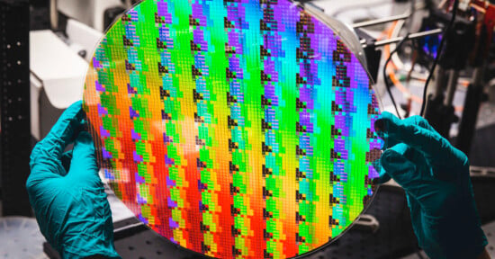
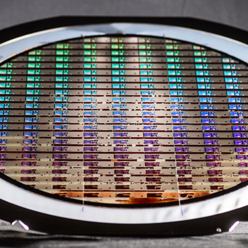
In an excellent report on Wired, Metalenz explains how it is ditching the idea of lens elements in groups, the defacto design of lenses for all cameras, and replacing them with a single lens built on a glass wafer that is between 1×1 to 3×3 millimeters in size. Under a microscope, the nanostructures on this wafer measure a scant one-thousandth the width of a human hair.
The claim is that those nanostructures are able to bend light the same way traditional multi-optic lens arrays do, and even correct for many of the shortcomings found in traditional lenses.
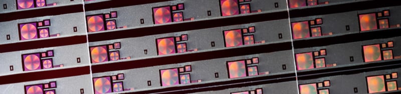
As light passes through these nanostructures, which make up the aforementioned optical metasurfaces, the result is similar to what is being done with curved sensors.
“Much in the way that a curved lens speeds up and slows down light to bend it, each one of these allows us to do the same thing, so we can bend and shape light just by changing the diameters of these circles,” Develin says.
Metalenz claims that the resulting image quality is just as sharp as what you would expect from traditional lens arrays but without the downsides of aberrations that occur when multiple lenses are stacked on one another. According to Wired, Metalenz has already partnered with two semiconductor leaders that are able to manufacture the optical metasurfaces at scale, which is important for a successful consumer rollout.
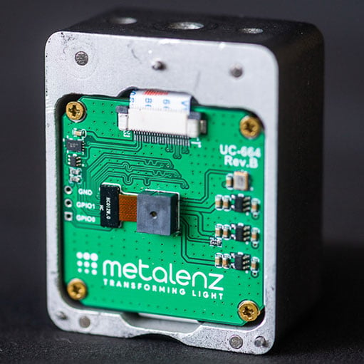
Metalenz says that it will go into mass production by the end of the year, and its first application will be a 3D sensor in a smartphone of a company it declined to name. The 3D sensor is similar to what is seen on Apple’s FaceID sensor, but because it doesn’t’ need to use lasers to illuminate a subject thanks to the increased light-gathering capabilities of the tech, Metalenz claims its product will be better at power conservation.
It’s unclear when an image-capture sensor by Metalenz will make its way to a consumer product, but if what the company claims is true, the camera bump may soon be a thing of the past.
(via Wired)